Linear Circuit Analyis (Webbook)
1. Introduction
2. Basic Concepts
- Charge, current, and voltage
- Power and energy
- Linear circuits
- Linear components
- Nodes and loops
- Series and parallel
- R, L & C combinations
- V & I combinations
3. Simple Circuits
- Ohm's law
- Kirchhoff's current law
- Kirchhoff's voltage law
- Single loop circuits
- Single node-pair circuits
- Voltage division
- Current division
4. Nodal and Mesh Analysis
5. Additional Analysis Techniques
- Superposition
- Source transformation
- The $V_{test}/I_{test}$ method
- Norton equivalent
- Thévenin equivalent
- Max power transfer
6. AC Analysis
7. Magnetically Coupled Circuits
8. Polyphase Systems
9. Operational Amplifiers
10. Laplace Transforms
11. Time-Dependent Circuits
- Introduction
- Inductors and capacitors
- First-order transients
- Nodal analysis
- Mesh analysis
- Laplace transforms
- Additional techniques
12. Two-Port Networks
Appendix
1. Introduction
1.1 Preface
Linear Circuit Analysis is a core course in electrical engineering that most undergraduate students need to take in the first year of their program. In fact, the course covers topics that are so fundamental that, most often, students from other engineering areas such as computer, industrial, power, or manufacturing engineering also need to take it as an introduction to electrical engineering.
This webbook is designed to be used by students to learn linear circuits while solving problems on the CircuitsU website; instructors can use the website to teach linear circuits without the need for other textbooks. This webbook and the problems generated by CircuitsU, cover most topics in the Linear Circuit Analysis course taught in undergraduate programs in the U.S. and is organized relatively similar to the existing textbooks on linear circuits.
The webbook is slightly different from other books or materials in linear circuits that you can find online. First, the webbook is written in a concise manner to make students spend a minimum amount of time learning the different topics on linear circuits and be able to spend more time practicing problems on their own. For this reason, just by browsing the pages of the webbook might not be sufficient to master all the topics on linear circuits (like a regular textbook is supposed to do) and students should first review the Examples of Solved Problems sections that appears at the end of most sections and then practice using the Practice Problems sections.
Second, the problems and examples that appear at the end of each section are generated randomly when the page is loaded, so students can look over and practice as many problems as they want. Due to the relatively large computational cost required to genearate random problems, you need to be logged in order to take advantage of the full set of examples and problems at the end of the sections.
Have fun!
1.2 Topics Covered in CircuitsU
Below is the list of topics for which CircuitsU can generate random problems, organized in chapters. The instructor can build homework assignments covering problems from different chapters (for instance, to design a midterm or a final exam). In addition, the instructor can change the type, difficulty, and number of homework problems that the site will generate in each homework assignment.
Chapters 1 and 2 provide an introduction to electric components, circuit diagrams, and concepts such as charge, current, voltage, energy and power in electric circuits. Chapters 3-10 focus on DC circuits; chapters 11-21 focus on AC circuits; chapters 22-26 focus on Laplace transforms and first and second-order transient circuits. These homework assignments cover most of the topics that are usually covered in a college-level, introductory course on linear circuit analysis. For instance, if the Linear Circuit Analysis course is taught as a:
- year-long course sequence: most topics could be covered throughout the course
- two-semester course sequence: chapters 1-16 could be offered during the first semester and chapters 17-26 are offered during the second semester
- three-quarter course sequence: chapters 1-10 could be offered during the first quarter, chapters 11-17 are offered during the second quarter, and chapters 18-26 are offered in the third quarter
Types of Problems
- General problems, in which students need to answer simple questions such as identifing different components in a circuit, or series and parallel connections.
- Numerical problems, (ℕ), in which the known variables in the problem are given numerically and students need to compute the shought variable or variables numerically.
- Analytical problems, (Ⓐ), in which the known variables are given symbolically and the students need to compute the analytically.
- Design problems, (ⅅ), in which students need to compute specific elements in a circuit in order for some conditions to be satisfied (e.g. what are the values of specific resistors such that the gain of an amplifier to be equal to 10).
- Graphical problems, (G), in which students need to extract information from a graphic and compute different quantities (e.g. compute the current going through a capacitor if the charge is given graphically as function of time).
1. Nodes and loops, series and parallel connections
- Identify resistors, capacitors, inductors, voltage and current sources in electric circuit diagrams
- Identify nodes and loops in electric circuits
- Identify series and parallel connections
2. Charge, current, voltage, energy, power
- Evaluate the charge going through a component
- Evaluate the energy generated or dissipated by a component
- Compute the instantaneous current, voltage, and power generated or dissipated
2. R, L, C combinations
- Compute the equivalent resistance of a network
- Compute the equivalent capacitance/inductance of a network of capacitors/inductors
- Compute the charge, current and voltage as a function of time in capacitors and inductors
- Compute the energy stored by capacitors and inductors
3. Simple circuits
- Use KVL and KCL to analyze single loop and single node-pair circuits
- Use voltage and current division to solve simple circuits
- Compute the power generated/dissipated by a component
4. DC nodal analysis
- Write and solve the system of nodal equations in DC circuits
- Compute DC currents, voltages, and powers using nodal analysis
- Use nodal analysis to solve design problems
5. DC mesh analysis
- Write and solve the system of mesh equations in DC circuits
- Compute DC currents, voltages, and powers using mesh analysis
- Use mesh analysis to solve design problems
6. DC superposition
- Analyze DC circuits using the method of superposition
7. DC source transformation
- Use source transformation to compute currents, voltages and powers in DC circuits
8. DC Norton and Thévenin equivalent circuits
- Compute the Norton and Thévenin equivalent circuits of a DC network
- Simplify DC circuits by making successive source transformations
9. Operational amplifiers (DC)
- Analyze DC circuits with ideal OpAmps
- Analyze DC circuits with real OpAmps (in which $A$, $R_{in}$ and/or $R_{out}$ are nonzero and finite
10. Impedance simplification (AC)
- Compute the equivalent (complex) impedance of a network containing resistors, capacitors and inductors
11. AC nodal analysis
- Write and solve the system of nodal equations in AC circuits
- Compute AC currents and voltages using nodal analysis
12. AC mesh analysis
- Write and solve the system of mesh equations in AC circuits
- Compute AC currents and voltages using mesh analysis
13. AC superposition
- Analyze AC circuits using the method of superposition
14. AC source transformation
- Use source transformation to compute currents and voltages in AC circuits
15. AC Norton and Thévenin equivalent circuits
- Compute the Norton and Thévenin equivalent circuits of an AC network
- Simplify AC circuits by making successive source transformations
16. Operational amplifiers (AC)
- Analyze AC circuits with ideal OpAmps
17. AC power analysis
- Calculate instantaneous and average power in AC circuits
- Calculate real power, reactive power, complex power, and power factor in AC circuits
- Find maximum power transfer
18. Magnetically coupled networks
- Analyze AC circuits with magnetically coupled inductors
- Analyze AC circuits with ideal transformers (nodal analysis, mesh analysis, transformer elimination)
19. Polyphase circuits
- Analyze two-phase and three-phase circuits
- Use delta-wye transformations
- Compute instantaneous and total power, and pf
20. Two-port networks
- Calculate the admittance ($y$), impedance ($z$), hybrid ($h$ and $g$), and transmission ($t$ and $t'$) parameters for two-port networks
- Convert from one type of network parameters to another type (e.g. $y$-parameters to $z$-parameters,...)
21. Frequency selective circuits
- Compute voltage gain ($G_v$), current gain ($G_i$), transimpedance ($Z$), and transadmittance ($Y$) of AC filters
- Compute the transfer function from a given Bode plot
- Draw the straight-line Bode magnitude plot for a specific transfer function
- Compute the resonant frequency, bandwidth, quality factor, half-power frequencies etc. in RLC circuits
22. Laplace transforms
- Compute the direct and inverse Laplace transforms of different functions using the linearity of Laplace transforms, time-shifting, frequency shifting, etc.
23. Laplace impedance simplification
- Transform a circuit from time domain to s-domain
- Compute the impedance of a circuit in the s-domain
24. First-order transient circuits
-
Compute time-dependent currents and voltages in first-order transient circuits using:
1) the time relaxation approach (aka step-by-step approach)
2) the Laplace transform method
3) the method of integro-differential equations (for nodal and mesh analysis)
25. Second-order transient circuits
-
Compute time-dependent currents and voltages in second-order transient circuits using:
1) the Laplace transform method
2) the method of integro-differential equations (nodal and mesh) analysis
26. Other applications of Laplace transforms
- Superposition in the s-domain
- Source transformation in the s-domain
- Norton and Thévenin equivalent circuits in the s-domain
- Higher-order transient circuits
1.3 Assignments by chapter
Below are the recommended assignments (HW1-HW32) that are generated by default when the instructor creates a new Linear Circuit Analysis course and choses Selected HW assignments by chapter (37 assignments).
| Module number | HW namea | HW numberb | Description |
|---|---|---|---|
| Module 1 | Series/Parallel | HW 1 | Identify R, L, C, voltage and current sources, nodes, and loops, series and parallel connections. |
| Module 2 | Charge, current, voltage, energy and power | HW 2 | Compute charge, currents, voltages, energy and power in single source-load networks. |
| Module 3 | Resistor simplification | HW 3 | Simplify a network of resistors using series and parallel transformations. |
| Module 4 | Simple circuits | HW 4 | Compute currents, voltages, and powers (dissipated and generated) in simple networks using KVL, KCL, current and voltage division. |
| Module 5 | DC nodal analysis (eqs.) | HW 5 | Write the system of nodal analysis equations (but do not solve it). |
| Module 6 | DC nodal analysis (num.) | HW 6 | Write and solve the system of nodal analysis equations to compute currents, voltages and powers. |
| Module 7 | DC mesh analysis (eqs.) | HW 7 | Write the system of mesh analysis equations (but do not solve it). |
| Module 8 | DC mesh analysis (num.) | HW 8 | Write and solve the system of mesh analysis equations to compute currents, voltages and powers. |
| Module 9 | DC superposition | HW 9 | Use the superposition method to compute currents and voltages in electric networks. |
| Module 10 | DC source transformation | HW 10 | Simplify a circuit using successive source transformations. |
| Module 11 | DC Norton/Thévenin | HW 11 | Compute the Norton and Thévenin equivalent circuits or DC networks. |
| Module 12 | DC OpAmps | HW 12 | Analyze circuits containing one or more operational amplifiers. |
| Module 14 | Inductors and capacitors | HW 14 | Current, voltage, charge, power and energy in inductors and capacitors; simplify networks of capacitors and inductors using series and parallel transformations. |
| Module 14 | Impedance simplification | HW 14 | Compute the effective impedance of an AC network of R, L, and C using series and parallel combinations. |
| Module 15 | AC nodal analysis | HW 15 | Compute currents and voltages in AC circuits using nodal analysis. |
| Module 16 | AC mesh analysis | HW 16 | Compute currents and voltages in AC circuits using mesh analysis. |
| Module 17 | AC superposition | HW 17 | Use the superposition method to compute currents and voltages in AC circuits. |
| Module 18 | AC source transformation | HW 18 | Simplify an AC circuit using successive source transformations. |
| Module 19 | AC Norton/Thévenin | HW 19 | Compute the Norton and Thévenin equivalent circuits or AC networks. |
| Module 20 | AC coupled inductors | HW 20 | Compute currents and voltages in AC networks containing coupled inductors using mesh analysis. |
| Module 21 | AC ideal transformers | HW 21 | Compute currents and voltages in AC networks containing ideal transformers using nodal or mesh analysis, or the transformer elimination method. |
| Module 22 | Polyphase circuits | HW 22 | Three-phase circuits, delta-wye transformations, power, and power factor. |
| Module 23 | RLC resonant circuits | HW 23 | Compute the resonant frequency, the quality factor, the band width, and half-power frequencies in RLC series and parallel circuits. |
| Module 24 | AC OpAmps | HW 24 | Single OpAmp inverters and followers containing AC sources, resistors, inductors, and capacitors. |
| Module 25 | AC power | HW 25 | Compute real power, reactive power, complex power, and power factor in AC circuits; power factor correction methods. |
| Module 26 | AC maximum power transfer | HW 26 | Compute maximum power transferred in AC circuits; AC power factor correction. |
| Module 27 | First-order transient circuits | HW 27 | Use the time relaxation approach to compute currents and voltages in first-order transient circuits. |
| Module 28 | Nodal analysis using ODEs (eqs.) | HW 28 | Write the system of nodal analysis ODEs for first, second and higher-order transient circuits (zero and non-zero initial conditions). |
| Module 29 | Mesh analysis using ODEs (eqs.) | HW 29 | Write the system of mesh analysis ODEs for first, second and higher-order transient circuits (zero and non-zero initial conditions). |
| Module 30 | Bode plots | HW 30 | Derive the transfer function from the Bode magnitude plot and draw the Bode magnitude plot of a transfer function. |
| Module 31 | Laplace transforms | HW 31 | Compute the direct Laplace transform of various functions. |
| Module 32 | Inverse Laplace transforms | HW 32 | Compute the inverse Laplace transform of various functions. |
| Module 33 | Laplace impedance simplification | HW 33 | Transform a circuit to s-domain and compute its equivalent s-domain impedance. |
| Module 34 | Laplace nodal analysis (num.) | HW 34 | Convert circuits to s-domain, then write and solve the system of nodal analysis equations for first and second-order transient circuits (zero initial conditions). |
| Module 35 | Laplace mesh analysis (num.) | HW 35 | Convert circuits to s-domain, then write and solve the system of mesh analysis equations for first and second-order transient circuits (zero initial conditions). |
| Module 36 | Source transformation in s-domain (num.) | HW 36 | Source transformations, Norton/Thévenin equivalent circuits and superposition in the s-domain (zero initial conditions). |
| Module 37 | Two-port networks | HW 37 | Compute y, z, h, and t parameters of DC and AC two-port networks. |
bThe default homework name when a new course is generated in CircuitsU.
cThe default homework number when a new course is generated in CircuitsU.
1.4 2-Semester Courseplan
Semester 1
Below are the default assignments (HW1-HW19) that are generated when the instructor creates a new Linear Circuit Analysis course and choses Semester 1 in a 2-semester course. The table shows the proposed due dates for each HW set but each instructor can set his or her own time schedule. The instructor can also re-organize the content and change the type, difficulty, and number of homework problems in each set.
| Week numbera | HW nameb | HW numberc | Dued | Description |
|---|---|---|---|---|
| Week 1 | Series/Parallel | HW 1 | End of 2nd week | Identify R, L, C, voltage and current sources, nodes, and loops, series and parallel connections. |
| Week 2 | Resistor simplification | HW 2 | End of 2nd week | Simplify a network of resistors using series and parallel transformations. |
| Week 2 | Charge, current, voltage, energy and power | HW 3 | End of 2nd week | Compute charge, currents, voltages, energy and power in single source-load networks. |
| Week 3 | Simple circuits (I) | HW 4 | End of 3rd week | Compute currents, voltages, and powers (dissipated and generated) in circuits with one source and one resistor. |
| Week 3 | Simple circuits (II) | HW 5 | End of 3rd week | Compute currents, voltages, and powers in circuits with 3 or more components, using KVL, KCL, resistor simplifications, current and voltage division. |
| Week 4 | DC nodal analysis (eqs.) | HW 6 | Beginnig of 5th week | Write the system of nodal analysis equations (but do not solve it). |
| Week 4 | DC nodal analysis (num.) | HW 7 | Beginnig of 5th week | Write and solve the system of nodal analysis equations to compute currents, voltages and powers. |
| Week 5 | DC mesh analysis (eqs.) | HW 8 | End of 6th week | Write the system of mesh analysis equations (but do not solve it). |
| Week 5 | DC mesh analysis (num.) | HW 9 | End of 6th week | Write and solve the system of mesh analysis equations to compute currents, voltages and powers. |
| Week 6 | Midterm 1 | |||
| Week 7 | DC superposition | HW 10 | Beginning of 8th week | Use the superposition method to compute currents and voltages in electric networks. |
| Week 7 | DC source transformation | HW 11 | End of 9th week | Simplify a circuit using successive source transformations. |
| Week 8 | DC Norton/Thévenin | HW 12 | End of 9th week | Compute the Norton and Thévenin equivalent circuits or DC networks. |
| Week 9 | DC OpAmps | HW 13 | End of 10th week | Analyze circuits containing one or more operational amplifiers. |
| Week 10 | Inductors and capacitors | HW 14 | End of 11th week | Current, voltage, charge, power and energy in inductors and capacitors; simplify networks of capacitors and inductors using series and parallel transformations. |
| Week 10 | Impedance simplification | HW 15 | End of 11th week | Compute the effective impedance of an AC network of R, L, and C using series and parallel combinations. |
| Week 11 | AC nodal analysis | HW 16 | Beginnig of 13h week | Compute currents and voltages in AC circuits using nodal analysis. |
| Week 12 | AC mesh analysis | HW 17 | Beginnig of 14th week | Compute currents and voltages in AC circuits using mesh analysis. |
| Week 13 | AC analysis | HW 18 | End of 14th week | Use superposition, Norton and Thévenin, and other AC analysis techniques (including time-domain/complex transformations) to solve AC problems. |
| Week 14 | Midterm 2 | |||
| Week 15 | AC OpAmps | HW 19 | End of 15th week | Single OpAmp inverters and followers containing AC sources, resistors, inductors, and capacitors. |
| Week 16 | Final exam | |||
aThe week when the topic is covered in class.
bThe default homework name when a new course is generated in CircuitsU.
cThe default homework number when a new course is generated in CircuitsU.
dThese are only the recommended due date, however, they need to be set by the instructor. Shorter homework assignments can have the same due date.
Semester 2
Below are the default assignments (HW1-HW17) that are generated when the instructor creates a new Linear Circuit Analysis course and choses Semester 2 in a 2-semester course.
| Week number | HW | HW number | Due | Description |
|---|---|---|---|---|
| Week 1 | AC power | HW 1 | Beginning of 3nd week | Compute real power, reactive power, complex power, and power factor in AC circuits; power factor correction methods. |
| Week 2 | AC maximum power transfer | HW 2 | Beginning of 3rd week | Compute maximum power transferred in AC circuits; AC power factor correction. |
| Week 3 | Magnetically coupled inductors | HW 3 | Beginning of 4rd week | Compute currents and voltages in AC networks containing coupled inductors using mesh analysis. |
| Week 3 | Ideal transformers | HW 3 | Beginning of 4rd week | Compute currents and voltages in AC networks containing ideal transformers using nodal or mesh analysis, or the transformer elimination method. |
| Week 4 | Polyphase circuits | HW 5 | Beginning of 5th week | Three-phase circuits, delta-wye transformations, power, and power factor. |
| Week 4 | RLC resonant circuits | HW 6 | End of 5th week | Compute the resonant frequency, the quality factor, the band width, and half-power frequencies in RLC series and parallel circuits. |
| Week 5 | First-order transient circuits | HW 7 | Beginning of 7th week | Use the time relaxation approach to compute currents and voltages in first-order transient circuits. |
| Week 6 | Midterm 1 | |||
| Week 7 | Nodal analysis using ODEs (eqs.) | HW 8 | Beginning of 9th week | Write the system of nodal analysis ODEs for first, second and higher-order transient circuits (zero and non-zero initial conditions). |
| Week 8 | Mesh analysis using ODEs (eqs.) | HW 9 | Beginning of 9th week | Write the system of mesh analysis ODEs for first, second and higher-order transient circuits (zero and non-zero initial conditions). |
| Week 9 | Laplace transforms | HW 10 | End of 10th week | Compute the direct Laplace transform of various functions. |
| Week 9 | Inverse Laplace transforms | HW 11 | End of 10th week | Compute the inverse Laplace transform of various functions. |
| Week 10 | Laplace impedance simplification | HW 12 | End of 11th week | Transform a circuit to s-domain and compute its equivalent s-domain impedance. |
| Week 10 | Nodal analysis in s-domain (num.) | HW 13 | End of 12th week | Convert circuits to s-domain, then write and solve the system of nodal analysis equations for first and second-order transient circuits (zero initial conditions). |
| Week 11 | Mesh analysis in s-domain (num.) | HW 14 | End of 12th week | Convert circuits to s-domain, then write and solve the system of mesh analysis equations for first and second-order transient circuits (zero initial conditions). |
| Week 12 | Source transformation in s-domain (num.) | HW 15 | Beginning of 13th week | Source transformations, Norton/Thévenin equivalent circuits and superposition in the s-domain (zero initial conditions). |
| Week 13 | Bode plots | HW 16 | Beginning of 14th week | Derive the transfer function from the Bode magnitude plot and draw the Bode magnitude plot of a transfer function. |
| Week 14 | Midterm 2 | |||
| Week 15 | Two-port networks | HW 17 | End of 15th week | Compute y, z, h, and t parameters of DC and AC two-port networks. |
| Week 16 | Final exam | |||
1.5 3-Quarter Courseplan
Quarter 1
Below are the default assignments (HW1-HW12) that are generated when the instructor creates a new Linear Circuit Analysis course and choses Quarter 1 in a 3-quarter course. The table shows the proposed due dates for each HW set but each instructor can set his or her own time schedule. The instructor can also re-organize the content and change the type, difficulty, and number of homework problems in each set.
| Week numbera | HW nameb | HW numberc | Dued | Description | |
|---|---|---|---|---|---|
| Week 1 | Series/Parallel | HW 1 | End of 2nd week | Identify R, L, C, voltage and current sources, nodes, and loops, series and parallel connections. | |
| Week 2 | Resistor simplification | HW 2 | End of 2nd week | Simplify a network of resistors using series and parallel transformations. | |
| Week 3 | Simple circuits (I) | HW 3 | End of 3rd week | Compute currents, voltages, and powers (dissipated and generated) in circuits with one source and one resistor. | |
| Week 3 | Simple circuits (II) | HW 4 | End of 3rd week | Compute currents, voltages, and powers in circuits with 3 or more components, using KVL, KCL, resistor simplifications, current and voltage division. | |
| Week 4 | DC nodal analysis (eqs.) | HW 5 | End of 4th week | Write the system of nodal analysis equations (but do not solve it). | |
| Week 4 | DC nodal analysis (num.) | HW 6 | End of 4th week | Write and solve the system of nodal analysis equations to compute currents, voltages and powers. | |
| Week 5 | DC mesh analysis (eqs.) | HW 7 | Beginning of 6th week | Write the system of mesh analysis equations (but do not solve it). | |
| Week 5 | DC mesh analysis (num.) | HW 8 | Beginning of 6th week | Write and solve the system of mesh analysis equations to compute currents, voltages and powers. | |
| Week 6 | Review session or optional midterm | ||||
| Week 7 | DC superposition | HW 9 | Beginning of 8th week | Use the superposition method to compute currents and voltages in DC networks. | |
| Week 7 | DC source transformation | HW 10 | Beginning of 9th week | Simplify a circuit using successive source transformations. | |
| Week 8 | DC Norton/Thévenin | HW 11 | Begining of 9th week | Compute the Norton and Thévenin equivalent circuits or DC networks. | |
| Week 9 | DC OpAmps | HW 12 | Beginning of 10th week | Analyze circuits containing one or more operational amplifiers. | |
| Week 10 | Final exam | ||||
aThe week when the topic is covered in class.
bThe default homework name when a new course is generated in CircuitsU.
cThe default homework number when a new course is generated in CircuitsU.
dThese are only the recommended due date, however, they need to be set by the instructor. Shorter homework assignments can have the same due date.
Quarter 2
Below are the default assignments (HW1-HW14) that are generated when the instructor creates a new Linear Circuit Analysis course and choses Quarter 2 in a 3-quarter course.
| Week number | HW name | HW number | Due | Description | |
|---|---|---|---|---|---|
| Week 1 | Inductors and capacitors | HW 1 | End of 2nd week | Current, voltage, charge, power and energy in inductors and capacitors; simplify networks of capacitors and inductors using series and parallel transformations. | |
| Week 2 | Impedance simplification | HW 2 | End of 2nd week | Compute the effective impedance of an AC network of R, L, and C using series and parallel combinations. | |
| Week 3 | AC nodal analysis | HW 3 | Beginnig of 4th week | Write the system of nodal analysis equations (but do not solve it). | |
| Week 3 | AC nodal analysis | HW 4 | Beginnig of 4th week | Write and solve the system of nodal analysis equations compute currents and voltages. | |
| Week 4 | AC mesh analysis | HW 5 | End of 5th week | Write the system of mesh analysis equations (but do not solve it). | |
| Week 4 | AC mesh analysis | HW 6 | End of 5th week | Write and solve the system of mesh analysis equations to compute currents and voltages. | |
| Week 5 | AC superposition | HW 7 | End of 6th week | Use the superposition method to compute currents and voltages in DC networks | |
| Week 5 | AC Norton/Thévenin | HW 8 | Beginning of 7th week | Compute the Norton and Thévenin equivalent circuits or AC networks. | |
| Week 6 | Review session or optional midterm | ||||
| Week 7 | AC analysis | HW 9 | Beginning of 8th week | Use a.c techniques to solve general AC circuits. | |
| Week 7 | AC OpAmps | HW 10 | Beginning of 8th week | Single OpAmp inverters and followers containing AC sources, resistors, inductors, and capacitors. | |
| Week 8 | AC power | HW 11 | Beginning of 9nd week | Compute real power, reactive power, complex power, and power factor in AC circuits; power factor correction methods. | |
| Week 8 | AC maximum power transfer | HW 12 | Beginning of 9th week | Compute maximum power transferred in AC circuits; AC power factor correction. | |
| Week 9 | AC coupled inductors | HW 13 | End of 9th week | Compute currents and voltages in AC networks containing coupled inductors using mesh analysis. | |
| Week 9 | AC ideal transformers | HW 14 | End of 9th week | Compute currents and voltages in AC networks containing ideal transformers using nodal or mesh analysis, or the transformer elimination method. | |
Quarter 3
Below are the default assignments (HW1-HW13) that are generated when the instructor creates a new Linear Circuit Analysis course and choses Quarter 3 in a 3-quarter course.
| Week number | HW name | HW number | Due | Description | |
|---|---|---|---|---|---|
| Week 1 | Polyphase circuits | HW 1 | End of 2nd week | Three-phase circuits, delta-wye transformations, power, and power factor. | |
| Week 1 | RLC resonant circuits | HW 2 | End of 2rd week | Compute the resonant frequency, the quality factor, the band width, and half-power frequencies in RLC series and parallel circuits. | |
| Week 2 | First-order transient circuits | HW 3 | End of 3th week | Use the time relaxation approach to compute currents and voltages in first-order transient circuits. | |
| Week 3 | Nodal analysis using ODEs (eqs.) | HW 4 | Beginning of 4th week | Write the system of nodal analysis ODEs for first, second and higher-order transient circuits (zero and non-zero initial conditions). | |
| Week 4 | Mesh analysis using ODEs (eqs.) | HW 5 | Beginning of 4th week | Write the system of mesh analysis ODEs for first, second and higher-order transient circuits (zero and non-zero initial conditions). | |
| Week 5 | Laplace transforms | HW 6 | Beginning of 6th week | Compute the direct Laplace transform of various functions. | |
| Week 5 | Inverse Laplace transforms | HW 7 | Beginning of 6th week | Compute the inverse Laplace transform of various functions. | |
| Week 6 | Review session or optional midterm | ||||
| Week 7 | Laplace impedance simplification | HW 8 | Beginning of 7th week | Transform a circuit to s-domain and compute its equivalent s-domain impedance. | |
| Week 7 | Nodal analysis in s-domain (num.) | HW 9 | End of 7th week | Convert circuits to s-domain, then write and solve the system of nodal analysis equations for first and second-order transient circuits (zero initial conditions). | |
| Week 8 | Mesh analysis in s-domain (num.) | HW 10 | End of 8th week | Convert circuits to s-domain, then write and solve the system of mesh analysis equations for first and second-order transient circuits (zero initial conditions). | |
| Week 8 | Source transformation in s-domain (num.) | HW 11 | Beginning of 9th week | Source transformations, Norton/Thévenin equivalent circuits and superposition in the s-domain (zero initial conditions). | |
| Week 9 | Bode plots | HW 12 | Beginning of 10th week | Derive the transfer function from the Bode magnitude plot and draw the Bode magnitude plot of a transfer function. | |
| Week 9 | Two-port networks | HW 13 | Beginning of 10th week | Compute y, z, h, and t parameters of DC and AC two-port networks. | |
| Week 10 | Final exam | ||||
1.6 Notations
This webbook and CircuitsU use the following notations:
| $I$, $V$, $P_d$, and $P_g$ | DC currents, voltages, and powers are denoted with capital letters |
| $I$, $V$, $P_d$, and $P_g$ | currents, voltages, and powers in the frequency (complex) and s-domains are denoted with capital letter* |
| $I(t)$, $V(t)$, $P_d(t)$, and $P_g(t)$ | time-dependent currents, voltages, and powers are usually shown as functions of time |
| $I(t)=I_0 \cos(\omega t+\phi)$ $V(t)=V_0\sin(\omega t+\phi)$ | AC currents AC voltages |
| $v_1$, $v_2$,... | nodal potentials (real, complex, or in the s-domain) are written in lowercases |
| $i_1$, $i_2$,... | mesh currents (real, complex, or in the s-domain) are written in lowercases |
| $v_1(t)$, $v_2(t)$,... | nodal potentials in time-domain |
| $i_1(t)$, $i_2(t)$,... | mesh currents in time-domain |
| $\class{mjblue}{j}$ | imaginary number $j=\sqrt{-1}$ |
| $\class{mjblue}{s}$ | complex frequency used in Laplace transforms |
| $\omega$ | angular frequency |
*A better notation, which is often used in textbooks, is to use bold letters for complex variables ($\boldsymbol{I}$, $\boldsymbol{V}$, $\boldsymbol{P_d}$, and $\boldsymbol{P_g}$) however, due to limitations in SVG graphic fonts the website uses regular fonts for both real and complex variables.
Subscripts
| $0$ | denotes sought variables (e.g. $V_0$, $I_0$) |
| $eff$ | effective (e.g. $R_{eff}$, $L_{eff}$,...) |
| $rms$ | root-mean square (e.g. $V_{rms}$, $I_{rms}$) |
| $d$ | dissipated (e.g. $P_d$) |
| $g$ | generated (e.g. $P_g$) |
| $N$ | Norton |
| $Th$ | Thévenin |
| $1$, $2$, ... | used for mesh currents (e.g. $i_1$, $i_2$,...), nodal potentials (e.g. $v_1$, $v_2$,...), components (e.g. $R_1$, $L_1$, $C_1$, $V_1$, $I_1$,...) |
| $x$, $y$, ... | used for control variables (e.g. $I_x$, $V_y$,...) |
Abbreviations
| AC | alternating current |
| DC | direct current (continuous current) |
| KCL | Kirchhoff's current law |
| KVL | Kirchhoff's voltage law |
| OpAmp | operational amplifier |
| TD | time-dependent |
Units
All variables are assumed to be expressed in the International System of Units in CircuitsU. Therefore, to simplify notations, CircuitsU will usually not write the units in mathematical expressions unless it is a final answer.
Units are written with gray characters in CircuitsU. For instance: $V_1 = 2.4 \: {\class{mjunit}{V}}$, $R = \frac{2.4 \: {\class{mjunit}{V}}}{1.2 \: {\class{mjunit}{A}}} =2 \: {\class{mjunit}{Ω}}$.
2. Basic Concepts
2.1 Electric Charge ($Q$)

Electric charge is a concept rigorously defined in electrostatics in terms of the properties matter exhibits when placed in an electromagnetic field. In the context of electric circuits, we are interested in the charge flowing through wires (or entering or leaving the terminal of a component). This charge equals the number of electrons passing through the wire ($N$) multiplied by the charge of a single electron ($-q$), where $q$ is the elementary charge: $$\begin{equation}q=1.602\times10^{-19}\:{\class{mjunit}C}\end{equation}$$
The SI unit of charge is the coulomb (${\class{mjunit}C}$). The name comes from the French physicist Charles-Augustin de Coulomb (1736–1806), who is best known for formulating Coulomb’s law, which describes the electrostatic force between two point charges $Q_1$ and $Q_2$: $$\begin{equation}F=\frac{1}{4\pi\epsilon_0} \cdot \frac{Q_1 Q_2}{r^2}\end{equation}$$ where $\epsilon_0$ is the electric permittivity of vacuum and $r$ is the distance between the two charges.
2.2 Electric Current ($I$)
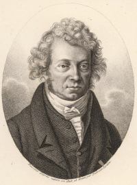
The electric current going through a wire is defined as the charge that goes through that wire in unit time $$\begin{equation}I(t)=\frac{dQ}{dt}\end{equation}$$ The SI unit of electric current is the ampere or amp (${\class{mjunit}A}$). The conventional symbol for current is $I$ (see Fig. 2.1), which originates from the French phrase intensité du courant, (current intensity). The $I$ symbol was first used by André-Marie Ampère (1775–1836), after whom the unit of electric current is named.
The current can flow in either of the two directions in a wire. When defining a variable $I$ to represent the current, the direction representing positive current must be specified, usually by an arrow on the wire. This is the reference direction of the current. The actual direction of current through a specific circuit element is usually unknown until the current is computed numerically or measured experimentally. Consequently, the reference directions of the currents are often assigned arbitrarily when we start analyzing a circuit. After the circuit is solved, a negative value for the current implies that the actual direction of the current is opposite than that of the reference direction.
If the current is known, one can compute the total charge that goes through the wire from time $t=0$ to $T$ by integrating the previous equation $$\begin{equation}Q(T)=\int_{0}^T I(t) dt\end{equation}$$
2.3 Electric Potential and Voltage ($V$)
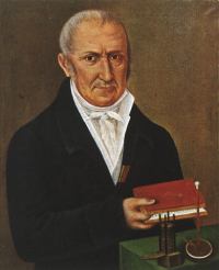
The electric potential, also known as electrostatic potential (or simply potential), is defined as the amount of work required to move a unit charge from a reference point (often taken at infinity) to a specified point. In electric circuit analysis, the reference point is conventionally chosen as the ground node, whose potential is assumed to be zero. The SI unit of electric potential is the volt (${\class{mjunit}V}$). The name comes from the Italian physicist Alessandro Volta (1745–1827), who invented the first chemical battery, known as the Voltaic pile.
Ideal wires are defined as wires with zero internal resistance. Therefore, the amount of work to move electrons from one point of an wire to another point of the same wire is equal to $0$. In addition, the electric potential of an ideal wire is the same at any point on the wire.
Voltage, also known as (electric) potential difference, is the difference of the electric potential between two points. Therefore, the SI unit of the voltage is the same as for electric potential, the volt. If we denote the two points by $A$ and $B$ and the potentials at those two points by $V_A$ and $V_B$, the voltage between the two points is $$\begin{equation}V_{AB}=V_{A}-V_{B}\end{equation}$$ To simplify the notations on circuit diagrams, we often denote point $A$ (the first point) with $+$ and point $B$ (the second point) with $-$ (see Fig. 2.1). In this case, voltage $V$ is understood to be the voltage from the node denoted with $+$ to the node denoted with $-$.
Finally, using the previous equation it is obvious that $$\begin{equation}V_{AB}=-V_{BA}\end{equation}$$
-
Analytical
Compute current when charge is given analytically
Compute charge when current is given analytically
Compute charge or current entering a box analytically
-
Graphical
Compute current when charge is given graphically (2 intervals)
Compute current when charge is given graphically (3 intervals)
Compute current when charge is given graphically (4 intervals)
Compute current when charge is given graphically (5 intervals)
Compute current when charge is given graphically (6 intervals)
Compute current when charge is given graphically (7 intervals)
Compute charge when current is given graphically (2 intervals)
Compute charge when current is given graphically (3 intervals)
Compute charge when current is given graphically (4 intervals)
Compute charge when current is given graphically (5 intervals)
Compute charge when current is given graphically (6 intervals)
Compute charge when current is given graphically (7 intervals)
Compute charge or current entering a box graphically (2 intervals)
Compute charge or current entering a box graphically (3 intervals)
Compute charge or current entering a box graphically (4 intervals)
Compute charge or current entering a box graphically (5 intervals)
Compute charge or current entering a box graphically (6 intervals)
Compute charge or current entering a box graphically (7 intervals)
2.4 Linear Circuits
Linear circuits are circuits that contain only linear components such as resistors, capacitors, inductors, ideal voltage and current sources, transformers, operational amplifiers, etc. Table 2.1 from the Linear components section presents a list of linear components together with their current-voltage characteristics. The current-voltage characteristics completely define the component for an electrical standpoint and, once these characteristics are known, one can completely predict how the component behaves in an electric circuit. In this course, we are focusing only on ideal components that do not break at higher voltages (in which case they would be considered non-linear).
Linear components of linear devices are those devices that have linear current-voltage characteristics. Intuitively, the current-voltage characteristic of a device is linear if it can be represented graphically by straight line on a current-voltage $V(I)$ or voltage-current $I(V)$ plot. Mathematically, a component is linear if for any currents $I_1$ and $I_2$ going through the device the voltage across the device satisfies $$\begin{equation} V(aI_1+bI_2)=aV(I_1)+bV(I_2) \end{equation}$$ or for any voltages $V_1$ and $V_2$ across the device the current going through the device satisfies $$\begin{equation} I(aV_1+bV_2)=aI(V_1)+bI(V_2) \end{equation}$$ where $a$ and $b$ are any real constants. It turns out that the analysis of linear circuits requires solving linear systems of equations, which can be algebraic equations with real or complex coefficients or linear ordinary differential equations.
Nonlinear circuits are circuits that contain at least one nonlinear component, which is a component in which the current-voltage characteristic is nonlinear. Examples of nonlinear components are diodes, transistors, and nonlinear sensors or actuators. Most often, real (practical) linear components such as voltage and current sources, resistors, transformers, etc. can be treated as linear on a small range of applied voltages and currents and they can become nonlinear if we increase this range. Nonlinear circuits can also be analyzed unsing Kirchhoff's laws, however, they will lead to systems of nonlinear equations that are usually more difficult to solve than systems of linear equations.
Importance
Linear circuits are also relatively easy to understand and study mathematically. Since they are linear, these circuits can be described by linear algebraic or differential equations, which can be always solved using simple algebra or linear differential equations theory. Unlike linear circuits, nonlinear circuits are described by nonlinear equations, which are usually more difficult to solve mathematically.
In practical applications, linear circuits are important because they do not distort the shape of the input signal. For this reason they can be used as amplifiers, voltage or current attenuators, linear sensors, etc.
Linear Components (Devices)
Table 2.1 shows a list of linear components (also called devices or elements) used in linear circuit analysis. All the components (and, implicitly, their current-voltage characteristics) are assumed to be ideal.
| Name/Unit | Symbol | Description |
|---|---|---|
| Resistor Ohms, $Ω$ |
Resistors
|
A resistor is a 2-terminal device that satisfies Ohm's law:$$\begin{equation}V(t)=I(t)R\end{equation}$$ where $R$ is the resistance and $V(t)$ is the voltage from the terminal where current $I(t)$ is assumed to enter the resistor to the terminal where the current is assumed to exit the resistor. In the case of DC circuits (i.e. when the voltage and current do not depend on time) the above equation is usually written as $V=IR$, where $V$ and $I$ are the DC values of the voltage and current. In the case of AC circuits (in frequency domain) the Ohm's law can be written in the same way, but $V$ and $I$ are the complex values of the voltage and current.
Why do resistors warm up? When current flows through a resistor, the moving charge carriers (usually electrons) collide with the atoms of the resistive material. These collisions impede the flow of electrons and convert part of the electrical energy into random thermal motion of the atoms — i.e., heat and possibly into light. This process in which the electrical energy is converted into heat is called Joule heating (or resistive heating). |
|
Capacitor Faradays, $F$ |
Ceramic and electrolytic capacitors
|
A capacitor is a 2-terminal device in which the current and voltage satisfy the following equation $$\begin{equation}I(t)=C\dfrac{dV(t)}{dt}\end{equation}$$ where $C$ is the capacitance (see figure for notations). Can the voltage across a capacitor change instantaneously? The answer is no, because doing so would cause the voltage across the inductor to become infinite (see the equation above). As a result, the current through an inductor cannot change instantaneously. In practice, one should always avoid sudden changes in the current through an inductor—for example, abruptly disconnecting the inductor from the circuit. In such a case, forcing the current to drop instantaneously from its initial value to zero can produce a very large voltage spike, potentially damaging the inductor or other circuit components. Instead, the energy stored in the inductor’s magnetic field will try to keep the current flowing, often discharging through a spark, arc, or protection device if no other path is provided. Capacitors can be divided into polarized and non-polarized types:
|
|
Inductor Henries, $H$ |
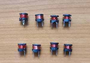
Inductors
|
An inductor is a 2-terminal device in which the current and voltage satisfy the following equation $$\begin{equation}V(t)=L\dfrac{dI(t)}{dt}\end{equation}$$ where $L$ is the inductance (see figure for notations). Can the current through an inductor change instantaneously? The answer is no, because doing so the voltage across the inductor would become infinite (see the equation above). As a result, the current through an inductor cannot change instantaneously. In practice, one should always avoid sudden changes in the current through an inductor—for example, suddently disconnecting the inductor from the circuit. In such a case, the current would decrease instantaneously from the initial value to 0, which could damage the inductor.. Can the current through an inductor change instantaneously? The answer is no, because doing so the voltage across the inductor would become infinite (see the equation above). As a result, the current through an inductor cannot change instantaneously. In practice, one should always avoid sudden changes in the current through an inductor—for example, suddently disconnecting the inductor from the circuit. In such a case, the current would decrease instantaneously from the initial value to 0, which could damage the inductor.. |
| Impedance Ohms, $Ω$ |
An impedance is a 2-terminal device that is defined in the frequency domain (i.e. in AC circuits) and in which the complex current and complex voltage satisfy the following equation $$\begin{equation}V=Z I\end{equation}$$ where $Z$ is the (complex) impedance (see figure for notations). Notice that the same symbol (rectangle) is sometimes used to represent a "black" box, which is an electronic component with two terminals that can contain a combinations of resistors, inductors, capacitors, sources, etc. | |
|
Voltage source (independent) Volts, $V$ |
An independent voltage source is a 2-terminal device in which the voltage from the positive to the negative terminals is always equal to $V$. The current flowing through a voltage source is generally unknown until the circuit is solved analytically (or the current is measured experimentally). If a voltage source is short-circuited, the circuit presents almost zero resistance to the source. As a result, the current rises dramatically, often far exceeding the source’s rated output. In general, this should never be done, as the excessive current can damage the source unless it is equipped with an appropriate protection mechanism. |
|
|
Current source (independent) Amperes, $A$ |
An independent current source is a 2-terminal device in which the current flowing in the direction of the arrow is always equal to $I$. The voltage accross a current source is generally unknown until the circuit is solved analytically (or the voltage is measured experimentally). Note that a current source adjusts the voltage across its terminals to maintain the current at its specified value. But what happens if a current source is disconnected from the circuit so that its terminals are left open? In practice, one should never do this, because with no path for current flow the source may develop an excessively high voltage and could be damaged unless it is equipped with a protection mechanism. |
|
| Dependent voltage source Volts, $V$ |
A dependent voltage source is a 2-terminal device in which the voltage from the positive to the negative terminals is equal to the value indicated ($V_x$ in this case), which can depend on other currents and voltages in circuit. | |
| Dependent current source Amperes, $A$ |
A dependent current source is a 2-terminal device in which the current flowing in the direction of the arrow is equal to the value indicated ($I_x$ in this case), which can depend on other currents and voltages in circuit. |
In addition to the linear components listed in Table 2.1, other examples of linear devices include transformers, operational amplifiers, and linear sensors. The first two of these components—transformers and operational amplifiers—will be studied in detail in later sections of this WebBook.
-
Identify resistors, capacitors, inductors, current and voltage sources in electric networks
Circuit with resistors, capacitors, inductors and independent sources
Circuit with resistors, capacitors, inductors, dependent and independent sources
2.5 Loops (meshes)
A loop (or mesh) is any closed path through the circuit in which nodes appear at most once. Meshes are defined in planar circuits, which are circuits that can be drawn on a plane surface with no wires crossing each other. Loops are slightly more general and can be applied to any circuit, planar or not. Since all the electric circuits that appear on this website are planar, we will use mesh and loop interchangeably.
A minor mesh (or minor loop) is a mesh that does not contain any other meshes. The outer mesh (or outer loop) of a circuit includes all the minor meshes in the circuit and is usually considered as a reference mesh.
A circuit can have multiple loops (or meshes). For instance, the circuit shown in Fig. 2.4 has 3 minor meshes labeled $i_1$, $i_2$, and $i_3$ and the outer mesh. Since, we are almost always interested only in the minor meshes and the outer mesh, we will simply say that that the circuit below contains 3 meshes (or 3 loops) plus the outer mesh (or outer loop).
Loops and meshes are made of branches.
Any circuit should contain at least one mesh. When the circuit contains only one mesh (which is the same as the outer mesh), it is called single loop circuit (see Fig. 2.5).
Mesh analysis is a method based on Kirchhoff's voltage law that can be used to analyze planar electric circuits. Loop analysis is slightly more general and can be applied to non-planar circuits. Mesh analysis is usually easier to use than loop analysis because the circuit is planar. However, notice again that, since all the electric circuits on this website are planar, we will use the names mesh analysis and loop analysis interchangeably.
-
Identify loops in electric networks
Circuit with 2 loops with resistors and a voltage source
Circuit with 4 loops with resistors, a voltage source and a current source
Circuit with 4-6 loops with resistors and dependent and independent sources
Circuit with 7-9 loops with resistors and dependent and independent sources
2.6 Nodes
A node is a collection of wires that are connected to each other. A circuit can have multiple nodes. For instance, the circuit shown in Fig. 2.6 has 5 nodes labeled $v_1$, $v_2$, $v_3$, $v_4$, and $v_5$.
Sometimes, one of the nodes is called the ground node. For instance, the circuits shown in Fig. 2.7 and Fig. 2.8 contain 4 nodes labeled $v_1$, $v_2$, $v_3$, and $v_4$, and the ground node (5 nodes in total). Notice that the two circuits have the same topology and the currents going through and the voltages across each component are the same.
Any circuit should contain at least 2 nodes (see Fig. 2.9). When the circuit contains only 2 nodes, it is called a single node-pair circuit.
Nodal analysis is a method based on Kirchhoff's current law that can be used to analyze electric circuits.
-
Identify nodes in electric networks
Circuit with 2 loops with resistors and a voltage source
Circuit with 4 loops with resistors, a voltage source and a current source
Circuit with 4-6 loops with resistors and dependent and independent sources
Circuit with 7-9 loops with resistors and dependent and independent sources
2.7 Series Connections
Two or more components (each with two terminals) are connected in series when they are part of the same two minor meshes, or, to one minor mesh and the outer mesh. For instance, in Fig. 2.10:
- Voltage source $V_1$ and resistor $R_1$ are connected in series because they both belong to minor mesh $i_1$ and the outer mesh.
- Current source $I_1$ and capacitor $C_1$ are connected in series because they both belong to minor mesh $i_3$ and the outer mesh.
- However, resistor $R_3$ and inductor $L_1$ are not connected in series because they belong to different pair of minor meshes (resistor $R_3$ belongs to $i_1$ and $i_2$, while inductor $L_1$ belongs to the outer mesh and $i_2$.
In Fig. 2.11:
- Voltage source $V_1$ and inductor $L_1$ are connected in series because they both belong to minor mesh $i_2$ and the outer mesh.
- Capacitor $C_1$, current source $I_1$ and capacitor $C_2$ are connected in series because they all belong to minor mesh $i_3$ and the outer mesh.
- Resistor $R_2$ and inductor $L_2$ are connected in series because they both belong to minor meshes $i_2$ and $i_3$.
If one component is connected in series with a second component, and the second component is connected in series with the third component, then the first component is also connected in series with the third component.
Parallel Connections
Two or more components (each having two terminals) are connected in parallel when they are connected between the same two nodes. For instance, looking at the circuit in Fig. 2.11:
- Capacitor $C_3$ and resistor $R_1$ are connected in parallel because they are both connected between nodes $v_2$ and $v_3$.
- However, inductors $L_1$ and $L_2$ are not connected in parallel because they are not connected between the same two nodes (inductor $L_1$ is connected between $v_3$ and $v_6$, while inductor $L_2$ is connected between $v_4$ and $v_6$).
If one component is connected in parallel with a second component, and the second component is connected in parallel with the third component, then the first component is also connected in parallel with the third component.
-
Identify series and parallel connections in electric networks
Circuit with 2 loops with resistors and a voltage source
Circuit with 4 loops with resistors, a voltage source and a current source
Circuit with 4-6 loops with resistors and dependent and independent sources
Circuit with 7-9 loops with resistors and dependent and independent sources
2.8 Resistor Combinations
Series
If two or more resistors $R_1$, $R_2$, ... $R_n$ are connected in series they are equivalent to a single resistor a resistor with $$\begin{equation}R_{eff}=R_1+R_2+...+R_n\end{equation}$$ That means we can replace one of the $n$ resistors with an equivalent resistor with resistance $R_{eff}$ and replace the other resistors with short-circuits (wires).
For instance, in Fig. 2.12, resistors $R_1$ and $R_2$ are connected in series. Therefore, we can keep one of the resistors, say $R_1$, replace its value with $R_{eff}=R_1+R_2$, and replace resistor $R_2$ with a wire.
Parallel
If two or more resistors $R_1$, $R_2$, ... $R_n$ are connected in parallel they are equivalent to a single resistor a resistor with $$\begin{equation}R_{eff}=\frac{1}{\frac{1}{R_1}+\frac{1}{R_2}+...+\frac{1}{R_n}}\end{equation}$$ That means we can replace one of the $n$ resistors with an equivalent resistor with resistance $R_{eff}$ and remove all the other resistors. When we have only two resistors connected in parallel, we can replace them with a single resistor with resistance $$R_{eff}=\frac{R_1 R_2}{R_1+R_2}$$
For instance, in Fig. 2.13, resistors $R_3$, $R_4$, and $R_5$ are connected in parallel. Therefore, we can keep one of the resistors, say $R_3$, replace its value with $R_{eff}=\frac{1}{\frac{1}{R_3}+\frac{1}{R_4}+\frac{1}{R_5}}$, and remove resistor $R_4$ from the circuit. Similarly, we could keep $R_4$ and remove $R_3$ and $R_5$, or keep $R_5$ and remove $R_3$ and $R_4$.
2.9 Inductor Combinations
Series
If two or more inductors $L_1$, $L_2$, ... $L_n$ are connected in series they are equivalent with a inductor with $$\begin{equation}L_{eff}=L_1+L_2+...+L_n\end{equation}$$ That means we can replace one of the $n$ inductors with an equivalent inductor with inductance $L_{eff}$ and replace the other inductors with short-circuits (wires).
For instance, consider the circuit in Fig. 2.14, in which inductors $L_1$ and $L_2$ are connected in series. In this circuit, we can keep one inductor, say $L_1$, replace its value with $L_{eff}=L_1+L_2$, and replace inductor $L_2$ with a wire.
Parallel
If two or more inductors $L_1$, $L_2$, ... $L_n$ are connected in parallel they are equivalent with a inductor with $$\begin{equation}L_{eff}=\frac{1}{\frac{1}{L_1}+\frac{1}{L_2}+...+\frac{1}{L_n}}\end{equation}$$ That means we can replace one of the $n$ inductors with an equivalent inductor with inductance $L_{eff}$ and remove all the other inductors. When we have only two inductors connected in parallel, we can replace them with a single inductors with inductance $$L_{eff}=\frac{L_1 L_2}{L_1+L_2}$$
For instance, consider the circuit in Fig. 2.15, in which inductors $L_3$, $L_4$, and $L_5$ are connected in parallel. In this circuit, we can keep one inductor, say $L_3$, replace its value with $L_{eff}=\frac{1}{\frac{1}{L_3}+\frac{1}{L_4}+\frac{1}{L_5}}$, and remove inductor $L_4$ from the circuit. Similarly, we could keep $L_4$ and remove $L_3$ and $L_5$, or keep $L_5$ and remove $L_3$ and $L_4$.
2.10 Capacitor Combinations
Series
If two or more capacitors $C_1$, $C_2$, ... $C_n$ are connected in series they are equivalent with a capacitor with $$\begin{equation}C_{eff}=\frac{1}{\frac{1}{C_1}+\frac{1}{C_2}+...+\frac{1}{C_n}}\end{equation}$$ That means we can replace one of the $n$ capacitors with an equivalent capacitor with capacitance $C_{eff}$ and replace the other capacitors with short-circuits (wires). When we have only two capacitors connected in parallel, we can replace them with a single capacitors with capacitance $$C_{eff}=\frac{C_1 C_2}{C_1+C_2}$$
For instance, consider the circuit in Fig. 2.16, in which capacitors $C_1$ and $C_2$ are connected in series. In this circuit, we can keep one capacitor, say $C_1$, replace its value with $C_{eff}=\frac{C_1 C_2}{C_1+C_2}$, and replace capacitor $C_2$ with a wire.
Parallel
If two or more capacitors $C_1$, $C_2$, ... $C_n$ are connected in parallel they are equivalent with a capacitor with $$\begin{equation}C_{eff}=C_1+C_2+...+C_n\end{equation}$$ That means we can replace one of the $n$ capacitors with an equivalent capacitor with capacitance $C_{eff}$ and remove all the other capacitors.
For instance, consider the circuit in Fig. 2.17, in which capacitors $C_3$, $C_4$, and $C_5$ are connected in parallel. In this circuit, we can keep one of the capacitors, say $C_3$, replace its value with $C_{eff}=C_3+C_4+C_5$, and remove capacitors $C_4$ and $C_5$ from the circuit. Similarly, we could keep $C_4$ and remove $C_3$ and $C_5$, or keep $C_5$ and remove $C_3$ and $C_4$.
-
Resistance simplifications (analytical)
Circuit with 2 loops, 4-6 resistors (analytical)
Circuit with 3 loops, 6 resistors (analytical)
Circuit with 5 loops, 8 resistors (analytical)
-
Resistance simplifications (numerical)
Circuit with 2 loops, 4-6 resistors (numerical)
Circuit with 3 loops, 6 resistors (numerical)
Circuit with 5 loops, 8 resistors (numerical)
Circuit with 8 loops, 13 resistors (numerical)
-
Inductance simplifications (analytical)
Circuit with 2 loops, 4-6 inductors (analytical)
Circuit with 3 loops, 6 inductors (analytical)
Circuit with 5 loops, 8 inductors (analytical)
-
Inductance simplifications (numerical)
Circuit with 2 loops, 4-6 inductors (numerical)
Circuit with 3 loops, 6 inductors (numerical)
Circuit with 5 loops, 8 inductors (numerical)
Circuit with 8 loops, 13 inductors (numerical)
-
Capacitance simplifications (analytical)
Circuit with 2 loops, 4-6 capacitors (analytical)
Circuit with 3 loops, 6 capacitors (analytical)
Circuit with 5 loops, 8 capacitors (analytical)
-
Capacitance simplifications (numerical)
Circuit with 2 loops, 4-6 resistor (numerical)
Circuit with 3 loops, 6 resistor (numerical)
Circuit with 6 loops, 8 resistor (numerical)
Circuit with 8 loops, 13 resistor (numerical)
2.11 Voltage Source Combinations
Series
If two or more voltage sources $V_1$, $V_2$, ... $V_n$ are connected in series they can be replaced with a single voltage source with $$V_{eff}=\pm V_1 \pm V_2\pm...\pm V_n$$ where the terms in the right-hand side are taken with $+$ sign if the corresponding voltage source $V_i$ is oriented in the same direction with $V_{eff}$ and with $-$ sign if $V_i$ is oriented in opposite direction with $V_{eff}$. Since the voltage sources are all connected in series, when we replace $V_i$ with $V_{eff}$, the other voltage sources are replaced with short-circuits (i.e. wires).
For instance, consider the circuit in Fig. 2.18, in which voltage sources $V_1$ and $V_2$ are connected in series (because they belong to both the outer loop and loop $i_1$). In this circuit, we can keep one voltage source, say $V_1$, replace its value with $$\begin{equation}V_{1,eff}=V_1-V_2\end{equation}$$ and replace voltage source $V_2$ with a wire. Notice that $V_1$ appears with a positive sign in the equation above because $V_1$ and $V_{1,eff}$ have the same polarity (i.e., orientation) relative to the reference loop $i_1$. In contrast, $V_2$ appears with a negative sign because $V_2$ and $V_{1,eff}$ have opposite polarities relative to the same reference loop $i_1$.
If we kept the other voltage source, $V_2$, we had to replace its value with $$\begin{equation}V_{2,eff}=V_2-V_1\end{equation}$$ (see figure below). In this case, $V_2$ was taken with positive sign because $V_2$ and $V_{2,eff}$ have the same polarity relative to the reference loop $i_1$, while $V_1$ as taken with a negative sign because its polarity is oposite to the polarity of $V_{1,eff}$ relative to the same reference loop $i_1$.
Parallel
Voltage sources should never be combined in parallel. What would happen if two voltage sources with different voltages are connected in parallel?
2.12 Current Source Combinations
Series
Current sources should never be combined in series. What would happen if we connect two current sources with different currents in series?
Parallel
If two or more current sources $I_1$, $I_2$, ... $I_n$ are connected in parallel they can be replaced with a single current source with $$I_{eff}=\pm I_1 \pm I_2\pm...\pm I_n$$ where the terms in the right-hand side are taken with $+$ sign if the corresponding current source $I_i$ points towards the same node as $I_{eff}$ and with $-$ sign if $I_i$ points to the other node. Since all the current sources are connected in parallel, when we replace $I_i$ with $I_{eff}$, the other current sources are removed (i.e. replaced with open circuits).
For instance, consider the circuit in Fig. 2.19, in which current sources $I_1$, $I_2$, and $I_3$ are connected in parallel. In this circuit, we can keep one current source, say $I_1$, replace its value with $$\begin{equation}I_{1,eff}=I_1-I_2+I_3\end{equation}$$ and remove current sources $I_2$ and $I_3$ from the circuit. Notice that $I_1$ and $I_3$ appear with positive sign in the above equation because both $I_1$ and $I_3$ point towards node $v_3$, just like $I_{1,eff}$. $I_2$ appears with negative sign because it points towards node $v_4$ while $I_{1,eff}$ points towards node $v_3$. If we kept current source $I_2$, we had to replace its value with $$\begin{equation}I_{2,eff}=-I_1+I_2-I_3\end{equation}$$ $I_1$ and $I_3$ appear with positive sign in the above equation because $I_2$ points towards node $v_4$, just like $I_{2,eff}$. $I_1$ and $I_3$ appear with negative sign because they point towards node $v_3$ while $I_{2,eff}$ points towards node $v_4$. Also, if we kept current source $I_3$, we had to replace its value with $$\begin{equation}I_{3,eff}=I_1-I_2+I_3\end{equation}$$
-
Combining voltage sources (analytical)
Circuit with 2 voltage sources, V0 (analytical)
Circuit with 3 voltage sources, V0 (analytical)
Circuit with 4 voltage sources, V0 (analytical)
Circuit with 5 voltage sources, V0 (analytical)
-
Combining voltage sources (numerical)
Circuit with 2 voltage sources (numerical)
Circuit with 3 voltage sources (numerical)
Circuit with 4 voltage sources (numerical)
Circuit with 5 voltage sources (numerical)
-
Combining current sources (analytical)
Circuit with 2 current sources, I0 (analytical)
Circuit with 3 current sources, I0 (analytical)
Circuit with 4 current sources, I0 (analytical)
Circuit with 5 current sources, I0 (analytical)
-
Combining current sources (numerical)
Circuit with 2 current sources (numerical)
Circuit with 3 current sources (numerical)
Circuit with 4 current sources (numerical)
Circuit with 5 current sources (numerical)
2.13 Power Dissipated

The power dissipated (also known as absorbed or consumed power) by a two-terminal component is given by
$$\begin{equation}P(t)=V(t) I(t)\end{equation}$$where voltage $V(t)$ and current $I(t)$ are shown in Fig. 2.20. Notice that we used the same sign convention for defining $V(t)$ and $I(t)$ as in Ohm's law. In general, power dissipation is time-dependent and varies with the instantaneous values of the voltage and current.
In general, the sign of the power dissipated by a component depends on the direction of current flow relative to the voltage polarity:
- If current flows from the positive terminal to the negative, it is supplying power (positive).
- If current flows from the negative terminal to the positive, it is absorbing power (negative).
In the case of resistors (that will be discussed in the next chapter), the power dissipated becomes $$\begin{equation}P(t)=R~\left[I(t)\right]^2=\frac{\left[V(t)\right]^2}{R}\end{equation}$$ where we used Ohm's law. Notice that, the power dissipated by a resistor is always non-negative (assuming that the resistance is positive). In the case of DC circuits, at steady-state, the power dissipated does not depend on time and $$\begin{equation}P=RI^2=\frac{V^2}{R}\end{equation}$$
The power dissipated by a component is measured in watts (${\class{mjunit}W}$). The name comes from the Scottish engineer James Watt (1736–1819), who made major improvements to the steam engine and helped usher in the Industrial Revolution.
Note: For the power absorbed by inductors and capacitors see Inductors and Capacitors.
2.14 Power Generated
The power generated (also known as produced power)) by a two-terminal component is defined as the negative of the power dissipated by that component
$$\begin{equation}P_g(t)=-P(t)=-V(t) I(t)\end{equation}$$where voltage $V(t)$ and current $I(t)$ are shown in Fig. 2.20.
The power generated by a component is measured in watts (${\class{mjunit}W}$).
2.15 Tellegen's Theorem
Consider an arbitrary lumped network that has $b$ branches and $n$ nodes. Suppose that to each branch we assign arbitrarily a branch potential difference $V_k(t)$ and a branch current $I_k(t)$ for $k=1,...,b$ that are measured with respect to arbitrarily picked associated reference directions. Tellegen's theorem states that $$\begin{equation}\sum_{k=1}^{b}{V_k(t) I_k(t)}=0\end{equation}$$
Tellegen's theorem can be proved using KVL and KCL and shows that the algebraic sum of the powers dissipated by an isolated electric circuit is equal to 0. In other words, the total power dissipated in a circuit is equal to the total power generated in the circuit. The theorem is a direct application of the law of conservation of energy and applies to any circuit with arbitrary elements, including linear, nonlinear, or time-varying components.
2.16 Energy Dissipated

The energy dissipated (also called absorbed or consumed) by a two terminal component from $t=0$ until $t=T$ is equal to $$\begin{equation}W(T)=\int_{0}^{T} \, V(t)I(t) \, dt\end{equation}$$
where voltage $V(t)$ and current $I(t)$ are shown in Fig. 2.21. Notice that, when we compute the power dissipated by a component, the current is defined as going from the positive to the negative terminal of the voltage definition.
At steady-state (in the case of DC circuits), the energy dissipated becomes $W=IVT$. Notice that the energy dissipated increases linearly with time.
The energy dissipated by a component is measured in joules (${\class{mjunit}J}$). The name comes from the English physicist James Prescott Joule (1818–1889), who investigated the relationship between heat, work, and mechanical energy.
Note: For the energy absorbed by (or stored in) inductors and capacitors see Inductors and Capacitors.
2.17 Energy Generated
The energy generated (also called produced) by a two terminal component is defined as the negative of the energy dissipated by that component $$\begin{equation}W_g=-W\end{equation}$$ and is also measured in joules (${\class{mjunit}J}$).
3. Simple Circuits
By simple circuits we understand those circuits that one should be able to solve relatively fast using simple circuit analysis techniques such as Ohm's law, current and voltage division, etc., without having to rely on more advanced methods such as nodal and mesh analysis. Examples of simple circuits are a battery that powers a DC motor, a few batteries in series that power a light bulb (such as a 3V-flashlight), a computer or TV that we connect to the AC power line, etc.
3.1 Ohm's Law
Ohm’s law states that the voltage across a resistor is directly proportional to the current going through the resistor. Denoting the constant of proportionality with $R$ (the resistance), one can express Ohm's law mathematically as $$\begin{equation}V=RI\end{equation}$$ or $$\begin{equation}I=\frac{V}{R}\end{equation}$$ where voltage $V$ and current $I$ are shown in Fig. 3.22. It is important to note that the value of the current calculated using Ohm’s law depends on how the voltage $V$ is defined. As shown in the figure, the current is assumed to flow from the $+$ node to the $–$ node; depending on the sign of $V$, this current can be either positive or negative.
If we introduce the conductance as the reciprocal of the resistance $G=\frac{1}{R}$, Ohm's law becomes $V=\frac{I}{G}$ or $I=GV$. (Please do not confuse conductance $G$ with gain $G$, which is a quantity that will be defined later in this webbook.)
The SI unit of resistance is ohm (${\class{mjunit}{Ω}}$). The name comes from the German physicist Georg Ohm (1789–1854), who formulated Ohm’s law, establishing the fundamental relationship between voltage, current, and resistance in an electrical circuit. The unit for conductance is siemens (${\class{mjunit}{S}}={\class{mjunit}{Ω^{-1}}}$), also known as mho (${\class{mjunit}{℧}}$).
-
Ohm's law (analytical)
Circuit with 1 resistor and 1 voltage source (analytical)
Circuit with 1 resistor and 1 current source (analytical)
Circuit with 2 resistors and 1 voltage source (analytical)
Circuit with 2 resistors and 1 current source (analytical)
-
Ohm's law (numerical)
Circuit with 2 resistors and 1 voltage source (analytical)
Circuit with 2 resistors and 1 current source (analytical)
Circuit with 1 resistor and 1 voltage source (numerical)
Circuit with 1 resistor and 1 current source (numerical)
-
Ohm's law (design)
Circuit with 1 resistor and 1 voltage source (numerical design)
Circuit with 1 resistor and 1 current source (numerical design)
Circuit with 2 resistors and 1 voltage source (numerical design)
Circuit with 2 resistors and 1 current source (numerical design)
3.2 Kirchhoff's Current Law (KCL)
Kirchhoff’s current law (KCL), also known as Kirchhoff’s first law or Kirchhoff’s junction rule, states that, for any node in an electrical circuit, the sum of currents flowing into the node is equal to the sum of currents flowing out of the node. In other words, the algebraic sum of currents at any node is zero (where we usually consider that current is signed positive if its direction is away from the node and negative if its direction is towards the node). Equivalently: $$\begin{equation}\sum_{i=1}^{n} I_i = 0\end{equation}$$ where $n$ is the total number of branches with currents flowing towards or away from the node. Notice that, in the case of time-dependent circuits, Kirchhoff’s current law holds at any moment in time and can be written as $\sum_{i=1}^{n} I_i(t) = 0$.
For instance, consider the circuit shown in Fig. 3.23. KCL, applied to the node shown in black, can be written as $$\begin{equation}I_{R_1}+I_{R_2}+I_{R_3}-I_2+I_{R_4}+I_1=0\end{equation}$$ Quite often, KCL is written in combination with Ohm's law in which case the current flowing through each resistor is expressed as the voltage across the resistor divided by the resistance.
Notice that KCL can also be written by considering that current is signed negative if its direction is away from a node and positive if its direction is towards the node. In this case, KCL becomes $$\begin{equation}-I_{R_1}-I_{R_2}-I_{R_3}+I_2-I_{R_4}-I_1=0\end{equation}$$ which is nothing else but the previous equation with all signs changed.
-
Kirchhoff's current law
Circuit with 1 resistor and 1 current source (analytical)
Circuit with 2 resistors and 1 current source (analytical)
Circuit with 1 resistor and 1 current source (numerical)
Circuit with 2 resistors and 1 current source (numerical)
Circuit with 1 resistor and 1 current source (numerical design)
Circuit with 2 resistors and 1 current source (numerical design)
3.3 Kirchhoff's Voltage Law (KVL)
Kirchhoff’s voltage law (KVL), also known as Kirchhoff’s second law or Kirchhoff’s loop rule, states that for any closed loop, the sum of the potential differences (voltages) across all components is zero: $$\begin{equation}\sum_{i=1}^{n} V_i = 0\end{equation}$$ where $n$ is the total number of voltages. Notice that, in the case of time-dependent circuits, Kirchhoff’s voltage law holds at any moment in time and can be written explicitly as $\sum_{i=1}^{n} V_i(t) = 0$.
For instance, consider the circuit shown in Fig. 3.24. If we go clockwise and add up the voltages across each component, KVL can be written as $$\begin{equation}R_1 I_0+V_2+R_2 I_0+V_3+R_5 I_0+R_4 I_0 + R_3 I_0-V_1=0\end{equation}$$ where we took the voltage of each source with positive sign if we went from the positive to the negative electrode and have applied Ohm's law when computing the voltage across each resistor. Notice that we can also write KVL by adding up the voltages going counterclockwise, in which case we have $$\begin{equation}-R_1 I_0+V_1-R_3 I_0-R_4 I_0-R_5 I_0-V_3 - R_2 I_0-V_2=0\end{equation}$$ however, the last two equations are identical if we move the terms to the right-hand side and reorder them.
If $I_0$ is taken in opposite direction (see Fig. 3.25), and we write KVL counter-clockwise, we have $$\begin{equation}R_1 I_0+V_1+R_3 I_0+R_4 I_0+R_5 I_0-V_3 + R_2 I_0-V_2=0\end{equation}$$
-
Kirchhoff's voltage law
Circuit with 1 resistor and 1 voltage source (analytical)
Circuit with 2 resistors and 1 voltage source (analytical)
Circuit with 1 resistor and 1 voltage source (numerical)
Circuit with 2 resistors and 1 voltage source (numerical)
Circuit with 1 resistor and 1 voltage source (numerical design)
Circuit with 2 resistors and 1 voltage source (numerical design)
3.4 Single Loop Circuits
Single loop circuits can usually be analyzed using Kirchhoff's voltage law (KVL) and Ohm's law. For instance, let us consider the circuit shown in Fig. 3.26, in which we need to compute current $I_0$.
Writing KVL clockwise (in the direction of current $I_0$) we have $$3I_0+5+2I_0+4+8I_0+1I_0+6I_0-7=0$$ which can be solved to obtain $$I_0= -\frac{2\ {\class{mjunit}{V}}}{20\ {\class{mjunit}{Ω}}}=-0.2\ {\class{mjunit}{A}} = -200\ {\class{mjunit}{mA}}$$
Notice that if we write KVL in opposite direction (but keet current $I_0$ as in Fig. 3.26), we would obtain the same answer for $I_0$.
-
Single loop circuits (analytical)
Circuit with 2 resistors and 1 voltage source (analytical)
Circuit with 4 resistors and 3 voltage sources (analytical)
Circuit with 4 resistors and 3 voltage sources (analytical)
Circuit with 4 resistors and 4 voltage sources, I0 (analytical)
Circuit with 4 resistors and 4 voltage sources, Pd (analytical)
Circuit with 4 resistors and 4 voltage sources, Pg (analytical)
-
Single loop circuits (numerical)
Circuit with 2 resistors and 2 voltage sources, I0 (numerical)
Circuit with 4 resistors and 3 voltage sources, I0 (numerical)
Circuit with 4 resistors and 3 voltage sources, V0 (numerical)
Circuit with 4 resistors and 4 voltage sources, I0 (numerical)
Circuit with 4 resistors and 4 voltage sources, Pd (numerical)
Circuit with 4 resistors and 4 voltage sources, Pg (numerical)
Circuit with 2 voltage sources (numerical)
Circuit with 3 voltage sources (numerical)
Circuit with 4 voltage sources (numerical)
Circuit with 5 voltage sources (numerical)
3.5 Single Node-Pair Circuits
Single node-pair circuits can typically be analyzed using Kirchhoff's current law (KCL) and Ohm's law. For instance, let us consider the circuit shown in Fig. 3.27, in which we need to compute voltage $V_0$.
Noticing that the voltage from the black (top) node to the red (bottom) node is $V_0$ and using Ohm's law, we can write KCL as $$\frac{V_0}{4}+\frac{V_0}{1}-7+\frac{V_0}{4}+2+\frac{V_0}{2}=0$$ which can be solved to obtain$$V_0= 10\ {\class{mjunit}{V}}$$
-
Single node-pair circuits (analytical)
Circuit with 2 resistors and 2 current sources, V0 (analytical)
Circuit with 4 resistors and 3 current sources, V0 (analytical)
Circuit with 4 resistors and 3 current sources, I0 (analytical)
Circuit with 4 resistors and 4 current sources, V0 (analytical)
Circuit with 4 resistors and 4 current sources, Pd (analytical)
Circuit with 4 resistors and 4 current sources, Pg (analytical)
Circuit with 1 resistors and 2 current sources, I0 (analytical)
Circuit with 1 resistors and 3 current sources, I0 (analytical)
Circuit with 1 resistors and 3 current sources, I0 (analytical)
Circuit with 1 resistors and 5 current sources, I0 (analytical)
-
Single node-pair circuits (numerical)
Circuit with 2 resistors and 3 current sources, V0 (numerical)
Circuit with 4 resistors and 3 current sources, V0 (numerical)
Circuit with 4 resistors and 3 current sources, I0 (numerical)
Circuit with 4 resistors and 4 current sources, V0 (numerical)
Circuit with 4 resistors and 4 current sources, Pd (numerical)
Circuit with 4 resistors and 4 current sources, Pg (numerical)
Circuit with 1 resistor and 2 current sources, I0 (numerical)
Circuit with 1 resistor and 3 current sources, I0 (numerical)
Circuit with 1 resistor and 4 current sources, I0 (numerical)
Circuit with 1 resistor and 5 current sources, I0 (numerical)
3.6 Voltage Division
Voltage division is a technique that can be used to compute the voltage across each resistor of a series combination of resistors when the voltage across all the resistors is known. For instance, if we have $n$ resistors connected in series and the total voltage across them is $V$, the voltage across resistor $R_i$ is equal to $$\begin{equation}V_i=V\frac{R_i}{R_1+R_2+...+R_n}\end{equation}$$
In the case of only two resistors, the previous equation gives $$\begin{equation}V_1=V\frac{R_1}{R_1+R_2}\end{equation}$$ $$\begin{equation}V_2=V\frac{R_2}{R_1+R_2}\end{equation}$$
Voltages $V_1$, $V_2$,... are defined such that their polarity is the same as the direction of voltage $V$. For instance, consider the circuit shown in Fig. 3.28.
Applying the voltage division equations we obtain $$V_{1}=20\ {\class{mjunit}{V}} \times\frac{2}{2+5+3}=4\ {\class{mjunit}{V}}$$ $$V_{2}=20\ {\class{mjunit}{V}} \times\frac{5}{2+5+3}=10\ {\class{mjunit}{V}}$$ $$V_{3}=-20\ {\class{mjunit}{V}} \times\frac{3}{2+5+3}=-6\ {\class{mjunit}{V}}$$ Notice that, in the last equation, $V_3$ has a negative sign because its defined polarity is opposite to the reference direction of the $20\ {\class{mjunit}{V}}$ source.
-
Voltage division
Circuit with 2 resistors and 1 voltage source (analytical)
Circuit with 3 resistors and 1 voltage source (analytical)
Circuit with 2 resistors and 1 voltage source (numerical)
Circuit with 3 resistors and 1 voltage source (numerical)
Circuit with 2 resistors and 1 voltage source (numerical design)
Circuit with 3 resistors and 1 voltage source (numerical design)
3.7 Current Division
Current division is a technique that can be used to compute the current going through each resistor of a parallel combination of resistors when the current going through all the resistors is known. In general, if we have $n$ resistors connected in parallel and the total current going through them is $I$, the current going through resistor $R_i$ is equal to $$\begin{equation}I_i=I\frac{\frac{1}{R_i}}{\frac{1}{R_1}+\frac{1}{R_2}+...+\frac{1}{R_n}}=I\frac{G_i}{G_1+G_2+...+G_n}\end{equation}$$ where $G_i=\frac{1}{R_i}$ is the conductance of each resistor. In the case of two resistors, the previous equation gives $$\begin{equation}I_1=I\frac{R_2}{R_1+R_2}\end{equation}$$ $$\begin{equation}I_2=I\frac{R_1}{R_1+R_2}\end{equation}$$
Currents $I_1$, $I_2$,... are defined such that their direction is the same as the direction of current $I$. For instance, consider the circuit shown in Fig. 3.29.
Applying the current division equations we obtain $$I_{1}=6\ {\class{mjunit}{A}} \times\frac{\frac{1}{8}}{\frac{1}{4}+\frac{1}{8}}=6\ {\class{mjunit}{A}} \times\frac{8}{4+8}=4\ {\class{mjunit}{A}}$$ $$I_{2}=-6\ {\class{mjunit}{A}} \times\frac{\frac{1}{4}}{\frac{1}{4}+\frac{1}{8}}=-6\ {\class{mjunit}{A}} \times\frac{4}{4+8}=-2\ {\class{mjunit}{A}}$$ Notice that, in the last equation, current $I_2$ has a negative sign because the current flows in opposite direction than the current induced by the $6\ {\class{mjunit}{A}}$ current source.
-
Current division
Circuit with 2 resistors and 1 current source (analytical)
Circuit with 3 resistors and 1 current source (analytical)
Circuit with 2 resistors and 1 current source (numerical)
Circuit with 3 resistors and 1 current source (numerical)
Circuit with 2 resistors and 1 current source (numerical design)
Circuit with 3 resistors and 1 current source (numerical design)
4. Nodal and Loop Analysis Techniques
4.1 Nodal Analysis
Nodal analysis is a method based on Kirchhoff's current law that can be used to compute the potentials in a circuit. The technique is based on the fact that, if a circuit has $n+1$ nodes (including the ground node), the $n$ potentials (excluding the potential of the ground node, which is assumed to be $0$) can be found by solving a system of $n$ independent equations that can be obtained by applying KCL, in which the current going through each branch is computed based on the current-voltage characteristic of the element on that branch. If the circuit contains $m$ voltage sources (notice that in the case of voltage sources, the current vs. voltage is a multivalued function), $m$ equations will be the voltage constrained equations of each voltage source as described below.
Algorithm
Assume we have a circuit with $n$ nodes (excluding the ground node), $m$ voltage sources and $c$ control variables.
- Identify the nodes in the circuit and select one of them as a reference node. The reference node is treated as ground node.
- Label the potentials at each of the $n$ nodes with $v_1$, $v_2$, ..., $v_n$, where $n$ is the number of nodes (excluding the ground node).
-
Write the system of nodal analysis equations, which will have $n+c$ equations ($m$ voltage constrained equations, $n-m$ KCL equations, and $c$ equations for the control variables). It is a good practice to write the $n+c$ equations in the order specified below:
A. Write $m$ voltage constrained equations. Write one voltage constrained equations for each voltage source $$\begin{equation}V_i=v_{i+}-v_{i-}\end{equation}$$ where $i=1,...,m$ and $v_{i+}-v_{i-}$ is the difference between the potentials of the positive and the negative electrodes of source $m$.
B. Write $c$ equations for control variables. Express each control variable (that usually appear in the definition of dependent sources) in terms of the $n$ nodal potentials.
C. Write KCL equations for regular nodes. Write KCL for each of regular node that does not connect a voltage source. When writing KCL, the current through each resistor (or impedance in the case of AC circuits) should be computed using Ohm's law.
D. Write KCL equations for supernodes. Write KCL for each supernode. As before, when writing KCL, the current through each resistor (or impedance) should be computed using Ohm's law.
- Solve the system on nodal analysis equations to compute the $n$ nodal potentials and $c$ control variables.
- Compute the sought variables.
Supernodes
-
A supernode is formed by enclosing (or combining) two or more nodes that are connected by one or more voltage sources; the combined nodes should not include the ground node.
Usually, we will need to write equations for supernodes whenever we have voltage sources that are not connected to the ground node directly of through any other voltage sources.
Since a supernode contains voltage sources, a supernode does not have a single potential (in fact, it will contain multiple regular nodes).
Fig. 4.30 shows an example of a circuit with one supernode formed by combining nodes $v_4$ and $v_5$. Note that the dependent voltage does not form a supernode because it is connected to ground through another voltage source ($V_1$). If $V_1$ was a resistor, the dependent source had formed another supernode. The KCL equation for the supernode shown in Fig. 4.30 is (notice that the crossed terms cancel each other) $$\begin{equation}\frac{v_4}{R_5}+\frac{v_5-v_3}{R_4}-I_1=0\end{equation}$$
Fig. 4.30 Example of a circuit with one supernode (shown in red). The two sources shown in blue do not form a supernode because they are connected to ground (either directly or through another voltage source). Fig. 4.31 shows an example of a circuit with one supernode formed by combining nodes $v_1$, $v_2$ and $v_4$. The KCL equation for the supernode shown in Fig. 4.31 is $$\begin{equation}\cancel{\frac{v_2-v_1}{R_1}}+\cancel{\frac{v_1-v_2}{R_1}}+\frac{v_1-v_3}{R_2}+\frac{v_2-v_3}{R_3}-\frac{v_5}{R_5}+=0\end{equation}$$
Fig. 4.31 Example of a circuit with one supernode (shown in red). - The number of KCL equations that we write at steps 3.C and 3.D is $n-m$.
- Sometimes, it is convenient to add the equations for the sought variables to the $n+c$ nodal analysis equations. In this case, the solution of the system will include contain the values of the sought variables.
- Nodal analysis can be used to analyze both linear and nonlinear circuits, DC and AC circuits, as well as time-dependent circuits. In the case of DC circuits we obtain a system of equations with real coefficients; in the case of AC circuits we obtain a system of equations with complex coefficients; in the case or time-dependent problems we obtain system of integro-differential equations (which can usually be reduced to a system of ordinary differential equations).
How to Compute the Sought Variables?
The sought variables can usually be expressed directly in terms of the nodal potentials.
- The voltage between two nodes can be expressed directly as the difference of the nodal potentials of the two nodes. For instance, the voltage $V_x$ in Fig. 4.30 is $V_x=0-v_4=-v_4$.
- The current going through a resistor can be computed using Ohm's law as a function of the voltage across the resistor and the resistance. For instance, the current going downwards through resistor $R_4$ in Fig. 4.31 is $(v_3-v_5)/R_4$.
- The current going out or in through a terminal of a voltage source can be computed indirectly, by writing KCL for the node which contains that terminal. In this way, we compute the sum of all currents entering and leaving the node, and by isolating the term associated with the voltage source we obtain the current flowing through its terminal. For instance, to compute current $I_0$ going through voltage source $V_2$ in Fig. 4.31, we can write that $$\begin{equation}I_0 = \frac{v_5-v_4}{R_4}-I_1\end{equation}$$
-
The power dissipated by a resistor can be found by computing the voltage across the resistor, say $V_R$, and using $P=V_R^2/R$. For instance, the power dissipated by resistor $R_1$ in Fig. 4.31 is $(v_1-v_2)^2/R_1$.
-
The power generated by a current source can be computed by multiplying the the current of the source by the voltage from node where the current goes out of the source to the node where current gets in the source. For instance, the power generated by source $I_1$ in Fig. 4.31 is $P_g=I_1(v_5-v_3)$
-
The power generated by a voltage source can be computed by multiplying the the voltage of the source by the current going from the negative to the positive terminal of the source. For instance, the power generated by source $V_2$ in Fig. 4.31 is $P_g=V_2\cdot(-I_0)$ (where $I_0$ was computed above).
-
DC nodal analysis (analytical)
Circuit with 2 nodes, 2 loops, 1 voltage source, 1 current source, 2 resistors (analytical): V0
Circuit with 3 nodes, 2 loops, 1 voltage source, 1 current source, 3 resistors (analytical): V0
Circuit with 3 nodes, 3 loops, 2 current sources, 4 resistors (analytical): I0
Circuit with 3 nodes, 3 loops, 1 voltage source, 1 current source, 4 resistors (analytical): I0
Circuit with 2 nodes, 2 loops, 1 voltage source, 1 current source, 2 resistors, 1 dependent source (analytical): V0
Circuit with 3 nodes, 3 loops, 1 voltage source, 1 current source, 4 resistors, 1 dependent source (analytical): V0&I0
Circuit with 4 nodes, 3 loops, 2 current sources, 5 resistors, (analytical): V0&I0&P
Circuit with 4 nodes, 3 loops, 1 voltage source, 1 current source, 5 resistors, 1 dependent source (analytical): V0&I0
Circuit with 5 nodes, 4 loops, 1 voltage source, 2 current sources, 6 resistors (analytical): V0&P
Circuit with 5 nodes, 4 loops, 2 voltage sources, 1 current source, 6 resistors (analytical): I0&P
Circuit with 5/6 nodes, 4 loops, 2 voltage sources, 1 current source, 6 resistors, 1 dependent source, supernode (analytical):
Circuit with 7 nodes, 6 loops, 2 voltage sources, 2 current sources, 9 resistors, 2 dependent sources, supernode (analytical):
-
DC nodal analysis (numerical)
Circuit with 2 nodes, 2 loops, 1 voltage source, 1 current source, 2 resistors (numerical): V0
Circuit with 3 nodes, 2 loops, 1 voltage source, 1 current source, 3 resistors (numerical): V0
Circuit with 3 nodes, 3 loops, 1 voltage source, 2 current sources, 4 resistors (numerical): I0
Circuit with 3 nodes, 3 loops, 1 voltage source, 1 current source, 4 resistors (numerical): V0&I0
Circuit with 2 nodes, 2 loops, 1 voltage source, 1 current source, 2 resistors, 1 dependent source (numerical): V0
Circuit with 3 nodes, 3 loops, 1 voltage source, 1 current source, 4 resistors (numerical): V0&I0&P
Circuit with 4 nodes, 3 loops, 2 current sources, 5 resistors (numerical): V0&P
Circuit with 4 nodes, 3 loops, 1 voltage source, 1 current source, 5 resistors (numerical): I0&P
Circuit with 5 nodes, 4 loops, 1 voltage source, 2 current source2, 6 resistors (numerical): V0&I0
Circuit with 5 nodes, 4 loops, 3 voltage source, 1 current source, 6 resistors, supernode (numerical): V0&I0
Circuit with 5/6 nodes, 4 loops, 2 voltage sources, 1 current source, 6 resistors, 1 dependent source, supernode (numerical): P
Circuit with 7 nodes, 6 loops, 2 voltage sources, 2 current sources, 9 resistors, supernode (numerical): P
4.2 Mesh Analysis
Mesh analysis is a method based Kirchhoff's voltage law that can be used to compute the currents flowing in each branch of a circuit. The technique is based on the fact that, if a circuit has $n$ minor meshes, the $n$ mesh currents can be found by solving a system of $n$ independent equations that can be obtained by applying KVL, in which the voltage across each component is computed based on its voltage-current characteristic. If the circuit contains $m$ current sources (notice that in the case of current sources the voltage vs. current is a multivalue function), $m$ equations will be the current constrained equations of each current source, as described below.
Algorithm
Assume we have a circuit with $n$ meshes (excluding the outer mesh), $m$ current sources and $c$ control variables.
- Identify the meshes in the circuit. The outer mesh is selected as a reference mesh (i.e. the mesh current of the outer loop is equal to 0).
- Label the currents at each of the $n$ meshes with $i_1$, $i_2$, ..., $i_n$.
-
Write the system of mesh analysis equations, which will have $n+c$ equations ($m$ current constrained equations, $n-m$ KVL equations, and $c$ equations for the control variables). It is a good practice to write the $n+c$ equations in the order specified below:
A. Write $m$ current constrained equations. Write one current constrained equations for each current source $$\begin{equation}I_i=i_{i1}+i_{i2}\end{equation}$$ where $i=1,...,m$ and $i_{i1}+i_{i2}$ is the algebraic sum of the two mesh currents adjacent to source $m$ going in reference with the direction of the current source. When all mesh currents are considered to be in the same direction (usually clockwise), one mesh current will usually enter with a plus sign, while the other with a minus sign in this formula.
B. Write $c$ equations for control variables. Express each control variable (that usually appear in the definition of dependent sources) in terms of the $n$ mesh currents.
C. Write KVL equations for regular meshes. Write KVL for each of regular mesh that does not connect a current source. When writing KVL, the current through each resistor (or impedance in the case of AC circuits) should be computed using Ohm's law.
D. Write KVL equations for supermeshes. Write KVL for each supermesh. As before, when writing KVL, the current through each resistor (or impedance) should be computed using Ohm's law.
- Solve the system on mesh analysis equations to compute the $n$ mesh currents and $c$ control variables.
- Compute the sought variables.
Supermeshes
-
A supermesh is a mesh formed by combining two or more meshes that include one or more current sources inside the combined mesh; the combined mesh cannot include any current source on its branches.
Usually, we need to write equations for supermeshes whenever we have current sources that are not part of the outer mesh and, by the combined mesh does not contain any current source on it borders.
Since a supermesh contains current sources inside itself, we cannot assign a single current to the supermesh.
Fig. 4.32 shows an example of a circuit with one supermesh. Current source $I_2$ results in a supermesh formed by combining $i_4$ and $i_5$. Notice that the combined supermesh is shown in red and does not contain any current sources on its branches. Current source $I_1$ does not result in a supermesh because the supermesh that it had created made by combining $i_1$ and $i_2$ would contain current source $2I_x$ on its branches. If the $2I_x$ source was a resistor, current source $I_1$ would result in another supermesh. The KVL equation for the supermesh shown in Fig. 4.32 is $$\begin{equation}V_1+i_5 R_5+(i_4-i_2)R_4=0\end{equation}$$
Fig. 4.32 Example of a circuit with one supermesh formed by combining meshes $i_4$ and $i_5$. Current source $I_1$ does not result in a supermesh, although it is not part of the outer mesh. - The number of KVL equations that we write at steps 3.C and 3.D is $n-m$.
- Sometimes, it is convenient to add the equations for the sought variables to the $n+c$ mesh analysis equations. In this case, the solution of the system will also contain the values of the sought variables.
- It is not mandatory to chose the outer mesh as a reference mesh. In principle, one could chose any mesh as the reference mesh and include the outer mesh as a regular mesh. However, this is almost never done in practice when solving mesh analysis problems.
- Mesh analysis can be used to analyze both linear and nonlinear circuits, DC and AC circuits, as well as time-dependent circuits. In the case of DC circuits we obtain a system of equations with real coefficients; in the case of AC circuits we obtain a system of equations with complex coefficients; in the case or time-dependent problems we obtain a system of integro-differential equations (which can usually be reduced to a system of ordinary differential equations).
How to Compute the Sought Variables?
The sought variables can usually be expressed directly in terms of the mesh currents.
- The current flowing through a branch of the circuit can be expressed as the difference of the neighboring two mesh currents. For instance, current $I_x$ in Fig. 4.32 is $I_x=i_4-i_3$.
- The voltage across a resistor can be computed using Ohm's law as a function of the current going through the resistor and the resistance. For instance, the voltage from left to right across resistor $R_1$ in Fig. 4.32 is $V_{R_1}=R_1 i_3$.
- The voltage across a current source can be computed indirectly, by writing KVL for a loop which contains the current source. In this way, we compute the sum of all the voltage drops around the loop, and by isolating the term associated with the current source we obtain its voltage. For instance, to compute voltage $V_0$ across current source $I_2$ in Fig. 4.32, we can write that $$\begin{equation}V_0 = I_5 R_5\end{equation}$$ Or, we can also write $$\begin{equation}V_0 = -V_1+(i_2-i_4)R_4\end{equation}$$
-
The power dissipated by a resistor can be found by computing the current going through the resistor, say $I_R$, and using $P=R I_R^2$. For instance, the power dissipated by resistor $R_3$ in Fig. 4.32 is $(i_1-i_3)^2/R_3$.
-
The power generated by a current source can be computed by multiplying the the current of the source by the voltage from node where the current goes out of the source to the node where current gets in the source. For instance, the power generated by source $I_2$ in Fig. 4.32 is $P_g=I_2\cdot(-V_0)$ (where $I_0$ was computed above).
-
The power generated by a voltage source can be computed by multiplying the the voltage of the source by the current going from the negative to the positive terminal of the source. For instance, the power generated by source $V_1$ in Fig. 4.32 is $P_g=V_1(i_3-i_4)$.
-
DC mesh analysis (analytical)
Circuit with 2 loops, 2 voltage sources, 3 resistors (analytical): I0
Circuit with 2 loops, 1 voltage source, 1 current source, 3 resistors (analytical): I0
Circuit with 2 loops, 1 voltage source, 1 current source, 3 resistors, 1 dependent source (analytical): V0
Circuit with 3 loops, 2 voltage sources, 4 resistors (analytical): I0&V0
Circuit with 3 loops, 1 voltage source, 1 current source, 4 resistors (analytical): I0&V0
Circuit with 3 loops, 1 voltage source, 1 current source, 4 resistors, 1 dependent source (analytical): I0&V0&P
Circuit with 3 loops, 1 voltage source, 1 current source, 4 resistors (analytical): I0&P
Circuit with 4 loops, 2 voltage sources, 1 current source, 5 resistors, 1 dependent source (analytical): V0&P
Circuit with 4 loops, 2 voltage sources, 1 current source, 6 resistors, supermesh (analytical): I0&P
Circuit with 5 loops, 2 voltage sources, 2 current sources, 6 resistors, 2 dependent sources, supermesh (analytical): P
Circuit with 6 loops, 2 voltage sources, 2 current sources, 9 resistors, 2 dependent sources, supermeshes (analytical): P
-
DC mesh analysis (numerical)
Circuit with 3 nodes, 2 loops, 2 voltage sources, 3 resistors (numerical): I0
Circuit with 3 nodes, 2 loops, 1 voltage source, 1 current source, 3 resistors (numerical): I0
Circuit with 3 nodes, 2 loops, 1 voltage source, 1 current source, 3 resistors, 1 dependent source (numerical): I0
Circuit with 3 nodes, 3 loops, 2 voltage sources, 4 resistors (numerical): V0
Circuit with 3 nodes, 3 loops, 1 voltage source, 1 current source, 4 resistors (numerical): V0
Circuit with 3 nodes, 3 loops, 1 voltage source, 1 current source, 4 resistors, 1 dependent source (numerical): I0
Circuit with 4 nodes, 4 loops, 2 voltage sources, 1 current source, 5 resistors (numerical): I0&V0
Circuit with 4 nodes, 4 loops, 2 voltage sources, 1 current source, 5 resistors, 1 dependent source (numerical): I0&V0
Circuit with 4 loops, 2 voltage sources, 1 current source, 6 resistors, supermesh (numerical): I0&P
Circuit with 5 loops, 2 voltage sources, 2 current sources, 6 resistors, 1 dependent source, supermesh (numerical): V0&P
Circuit with 6 loops, 2 voltage sources, 2 current sources, 9 resistors, 2 dependent sources, supermeshes (numerical): P
-
DC mesh analysis (numerical)
Circuit with 3 nodes, 2 loops, 2 voltage sources, 3 resistors (numerical design): V0&I0
Circuit with 3 nodes, 2 loops, 1 voltage source, 1 current source, 3 resistors (numerical design): V0&I0
Circuit with 3 nodes, 2 loops, 1 voltage source, 1 current source, 3 resistors, 1 dependent source (numerical design): V0&I0
Circuit with 3 nodes, 3 loops, 2 voltage sources, 4 resistors (numerical design): V0&I0
Circuit with 3 nodes, 3 loops, 1 voltage source, 1 current source, 4 resistors (numerical design): V0&I0
Circuit with 3 nodes, 2 loops, 1 voltage source, 1 current source, 4 resistors, 1 dependent source (numerical design): V0&I0
Circuit with 4 nodes, 4 loops, 2 voltage sources, 1 current source, 5 resistors (numerical design): I0&V0
Circuit with 4 loops, 2 voltage sources, 1 current source, 5 resistors, 1 dependent source (numerical design): I0&V0
Circuit with 4 loops, 2 voltage sources, 1 current source, 6 resistors, 1 dependent source (numerical design): I0&V0
Circuit with 5 loops, 1 voltage source, 1 current source, 6 resistors, 1 dependent source, supermesh (numerical design): I0&V0
Circuit with 6 loops, 2 voltage sources, 2 current sources, 9 resistors, 2 dependent sources, supermeshes (numerical design): I0&V0
5. Additional Analysis Techniques
5.1 Superposition
Superposition is a technique used to analyze linear electric circuits with multiple independent sources. It is based on the principle that the voltages and currents in such a circuit can be found by algebraically summing the voltages and currents produced by each independent source acting alone, with all other independent sources disabled (or set to zero).
Example 1
For instance, consider the circuit shown in Fig. 5.33(a), in which the sought variable is $I_0$. Using the principle of superposition we can write $I_0$ as a superposition of $I_{01}$ and $I_{02}$, where the latter can be computed using the circuits in Fig. 5.33(b) and Fig. 5.33(c). Using KVL and current division we have $$\begin{equation}I_0=I_{01}+I_{02}=-\frac{10}{2+3}+4\cdot\frac{2}{2+5}=-2+1.6=-0.4\ {\class{mjunit}A}\end{equation}$$
Example 2
Let us now consider the circuit shown in Fig. 5.34(a), which contains both dependent and independent sources and let us compute $I_0$. Using the principle of superposition we can write $I_0=I_{01}+I_{02}$, where $I_{01}$ and $I_{02}$ can be computed using the circuits in Fig. 5.34(b) and Fig. 5.34(c). Since these circuits contain both dependent and independent sources, we should normally solve them using nodal or mesh analysis. For instance, applying KVL in Fig. 5.34(b) we get $10+3I_{01}+3I_{01}+2I_{x1}=0$, which gives $I_{01}=-1.25\ {\class{mjunit}A}$. Applying mesh analysis for the circuit in Fig. 5.34(c) we have $I_{02}=4+I_{x2}$ and $3I_{02}+2I_{x2}+3I_{x2}=0$, which can be solved for $I_{02}=2.5\ {\class{mjunit}A}$. Hence: $$\begin{equation}I_0=I_{01}+I_{02}=-1.25+2.5=1.25\ {\class{mjunit}A}\end{equation}$$ and current $I_x$ from Fig. 5.34(a) becomes $$\begin{equation}I_x=I_0-4\ {\class{mjunit}A}=-2.75\ {\class{mjunit}A}\end{equation}$$
Algorithm
Assume we have a circuit that contains $n \ge 2$ independent sources and $m$ dependent sources and the sought variable is a current or voltage in the circuit. To compute the sought variable we split the circuit into a superposition of $n$ circuits, in which we activate only one independent source at a time.
- Keep only one independent source and deactivate all other independent sources. Notice that if the circuit contains dependent sources you need to keep those in the circuit (in a way, they are treated like resistors).
- Calculate the potentials and currents in the circuit.
- Repeat the last two steps for each source in the circuit.
- Superimpose the values of potentials and currents obtained at Step 2; pay special attention to the direction of the voltage drops and current flows.
Miscellaneous
- To deactivate a current source we remove it from the circuit (replace it with open-circuit or break); to deactivate a voltage source we replace it with a short-circuit (or wire).
- Unlike mesh and nodal analysis that can be applied to both nonlinear and linear circuits, superposition can be applied only to linear circuits. Therefore, in general, we cannot use superposition to compute the potential and currents in a circuit containing diodes, transistors, or other nonlinear elements.
- Special attention needs to be paid when computing the power using the method of superposition. If we need to compute the power generated or dissipated by a component, we need to compute the voltage across and the current flowing through that component, and then multiply the two to obtain the power.
- Superposition can be applied to circuits containing both dependent and independent sources. In this case superposition is applied only to the independent sources, while the dependent sources are always kept in the circuit.
It is clear from the two examples above that superposition can be easier to apply than nodal or mesh analysis when the circuit has no dependent sources (as in Fig. 5.33). In such cases, simple methods like resistor simplification and current or voltage division can be used to find the desired quantities in each superimposed circuit. However, if dependent sources are present (as in Fig. 5.34), we may still need to use nodal or mesh analysis to solve the superimposed circuits. In this situation, it is often simpler to solve the original circuit directly using nodal or mesh analysis.
5.2 Can Superposition Be Applied to Dependent Sources?
In the previous section we saw that superposition can be applied to circuits containing both independent and dependent sources (see Example 2 and Fig. 5.34). When we apply superposition to circuits containing dependent sources, we normally keep the dependent sources in the circuit at all times, while we deactivate only the independent sources one at a time. Therefore, if the circuit contains $n$ independent sources and $m$ dependent sources, we end up with $n$ circuits, each containing all $m$ dependent sources and only one independent source activated.
The question now is, can we apply superposition to dependent sources as well (like in Fig. 5.35 - notice that Fig. 5.35(b) and (c) do not contain the dependent source, while Fig. 5.35(d) contains only the dependent source)? In other words, can we write the original circuit as a superposition of $n+m=2+1=3$ circuits? Despite what is often suggested in the literature, the answer is YES, however, you need to do it carefully. For more information about this topic please refer to this paper by W. Marshall Leach from Georgia Tech.
Example 3
Consider again the circuit from Example 2, but now solve it using the superposition of dependent sources (see figure below).
Let us compute current $I_x$ using the superposition of dependent sources. Using Ohm's law, current division, and KVL, it is easy to show that
- $I_{x1} = -\frac{10}{2+3}=-2\ {\class{mjunit}A}$
- $I_{x2} = -4\cdot\frac{3}{2+3}=-2.4\ {\class{mjunit}A}$
- $I_{x3} = -\frac{3I_{x3}}{2+3}$
-
DC superposition (analytical)
Circuit with 2 loops, 1 voltage source, 1 current source, 2 resistors (numerical)
Circuit with 3 loops, 2 voltage sources, 4 resistors (numerical)
Circuit with 3 loops, 2 curent sources, 4 resistors (numerical)
Circuit with 3 loops, 1 voltage source, 1 current source, 4 resistors (numerical)
Circuit with 3 loops, 3 sources, 4 resistors (numerical)
Circuit with 4 loops, 3 sources, 4 resistors (numerical)
Circuit with 3 loops, 3 sources, 4 resistors (numerical)
Circuit with 4 loops, 3 sources, 4 resistors (numerical)
-
DC superposition (numerical)
Circuit with 2 loops, 1 voltage source, 1 current source, 2 resistors (analytical)
Circuit with 3 loops, 2 voltage sources, 4 resistors (analytical)
Circuit with 3 loops, 2 current sources, 4 resistors (analytical)
Circuit with 3 loops, 1 voltage source, 1 current source, 4 resistors (analytical)
Circuit with 3 loops, 3 sources, 4 resistors (analytical)
Circuit with 4 loops, 3 sources, 4 resistors (analytical)
Circuit with 3 loops, 3 sources, 4 resistors, 1 dependent source (analytical)
Circuit with 4 loops, 3 sources, 4 resistors, 1 dependent source (analytical)
- For problems with AC Superposition AC Analysis Methods section. For problems with Superposition in the s-domain Additional in Time-Dependent Circuits Techniques in Time-Dependent Circuits section.
5.3 Source Transformation
Source transformation is the process of modifying a linear circuit by transforming voltage sources into current sources using Norton's theorem, and vice versa using Thévenin's theorem. The process is usually combined with series and parallel simplifications of resistor (or impedance in the case of AC circuits), current sources and voltage sources in order o simplify the original circuit or compute the thought variable.
Source transformation can be applied to both independent and dependent sources.
Conversion from Norton to Thévenin Equivalent Circuit
When transforming a circuit from a Norton equivalent circuit to a Thévenin equivalent circuit the value of the resistance remains the same, while the voltage of the voltage source is $$\begin{equation}V=R I\end{equation}$$
Conversion from Thévenin to Norton Equivalent Circuit
When transforming a circuit from a Thévenin equivalent circuit to a Norton equivalent circuit the value of the resistance remains the same, while the current of the current source is $$\begin{equation}I=\frac{V}{R}\end{equation}$$
Simple Example
Consider the circuit shown in Fig. 5.38(a), where we need to determine the current $I_x$. If we start by performing a source transformation on the independent voltage source, we would lose the variable of interest, which also serves as the control variable for the dependent source. Therefore, we begin by applying the source transformation to the dependent voltage source instead. This source can be replaced by an equivalent current source with current $\frac{3I_x}{3} = I_x$, as illustrated in Fig. 5.38(b).
Notice that, consistent with the convention established in Fig. 5.37, the current of the transformed source is directed away from
the source and toward the node where the positive terminal of the original voltage source was connected. It is important to follow this convention every
time we perform a source transformation.
Finally, we can combine the two voltage sources and the resistors and obtain the circuits shown in Fig. 5.39(5). Since this is a simple circuit (which contains only one loop), we can compute the sought variable by writting KVL $$\begin{equation}23+3I_x + 5I_x =0\end{equation}$$ which can be solved for $$\begin{equation}I_x=-\frac{23}{8}=2.75\ {\class{mjunit}V}\end{equation}$$ which is the same value as the one obtained in Example 3 in the Superposition section.
-
DC source transformation (numerical)
Circuit with 2 loops, 2 sources, 2-3 resistors (numerical simplification)
Circuit with 3 loops, 2 sources, 3 resistors (numerical simplification)
Circuit with 4 loops, 3 sources, 4 resistors (numerical simplification)
Circuit with 5 loops, 3 sources, 6 resistors (numerical simplification)
- For problems with AC Source Transformation AC Analysis Methods section. For problems with Source Transformation in the s-domain Additional in Time-Dependent Circuits Techniques in Time-Dependent Circuits section.
5.4 The $V_{test}/I_{test}$ method
Have you ever wondered how an ohmmeter works (an ohmmeter is an instrument that measures the resistance or impedance of a circuit)? In order to measure the resistance of a network the ohmmeter applies a small voltage at the terminals of the network and measures the current going through the terminals. Then, it uses Ohm's law to compute the resistance of the circuit. This principle stays at the basis of the $V_{test}/I_{test}$ method that is often used in electronics to measure or compute the resistance of a network. Depending on the type of the source that is used to energize the network, we distinguish two methods.
The Test Voltage Source Method
When using the test voltage source method we apply a test voltage (in theoretical calculations often taken equal to $1 \: {\class{mjunit}V}$) and compute the value of the current injected by this source. Then, the resitance of the network is comptued using
$$\begin{equation}R=\frac{V_{test}}{I_{test}}\end{equation}$$The Test Current Source Method
When using the test current source method we apply a test current (in theoretical calculations often taken equal to $1 \: {\class{mjunit}A}$) and compute the value of the voltage at the terminals of the network. Then, the resitance of the network is comptued using the same equation as above.
Notes
- Whenever you use the $V_{test}/I_{test}$ method to determine the resistance of a circuit, you need to make sure your circuit does not have any independent sources that could affect your measurements (in practice they can damage your ohmmeter).
- The $V_{test}/I_{test}$ method is often used to determine the Norton and Thévenin resistance (or impedance in the case of AC circuits) of a network.
-
DC Norton & Thévenin circuits (analytical)
Circuit with 2 loops, 1 source, 3 resistors (analytical Thévenin and Norton)
Circuit with 3 loops, 1 voltage source, 1 current source, 3 resistors (analytical Thévenin and Norton)
Circuit with 3 loops, 1 voltage source, 1 current source, 3 resistors, 1 independent source (analytical Thévenin and Norton)
Circuit with 3 loops, 4 resistors, 1 dependent source (analytical Thévenin and Norton)
-
DC Norton & Thévenin circuits (numerical)
Circuit with 2 loops, 1 source, 3 resistors (numerical Thévenin and Norton)
5.5 Norton's Theorem
Norton's theorem states that any two-terminal linear circuit containing voltage sources, current sources and resistors (or impedances and transformaers in the case of AC circuits) can be replaced by an equivalent combination of a current source $I_{N}$ in parallel with a resistor $R_{N}$ (or impedance $Z_{N}$ in the case of AC circuits).
Norton's theorem and its dual, Thévenin's theorem, are widely used to simplify circuit analysis and study a circuit's initial-condition and steady-state response. Norton's theorem may in some cases be more convenient to use than Kirchhoff's circuit laws when analyzing linear circuits.
Calculating the Norton Equivalent Circuit
Calculating the Norton equivalent circuit, or simply the Norton equivalent of a circuit with two terminals means computing the Norton current and Norton resistance of the circuit.
The Norton current can be computed using any of the following methods:
- $I_{N} = I_{s.c}$ - the Norton current is equal to the short-circuit current at the output terminals of the original circuit. To compute $I_{s.c.}$ one can use any of the methods of linear circuit analysis such as nodal analysis, mesh analysis, or current and voltage division.
- If the Thévenin voltage $V_{Th}$ and Thévenin resistance $R_{Th}$ are known and $R_{Th} \neq 0$, one can calculate the Norton current using $I_{N} = V_{Th}/R_{Th}$ .
The Norton resistance can be computed using any of the following methods:
- $R_{N}$ can be computed by deactivating all independent sources and using the test voltage or test current methods using Ohm's law, $R_{N}=\frac{V_{test}}{I_{test}}$. To use the test voltage method, we connect a test voltage source at the output terminals (usually, but not necessarily, taken as $V_{test}=1~V$) and compute current $I_{test}$. To use the test current method, we connect a test current source at the output terminals (usually, but not necessarily, taken as $I_{test}=1~A$) and compute voltage $V_{test}$.
- If the circuit does not contain any dependent sources, $R_{N}$ can be computed by deactivating all independent sources and looking at the resistance seen from the output terminals (in this case, $R_{N}$ can often be computed using series and parallel simplifications of resistors).
- If $I_N$ and $V_{Th}$ are known and $I_{N} \neq 0$, one can calculate the Norton resistance using $R_{N} = \frac{V_{Th}}{I_{N}}$. However, please note that if $I_{N}=0$, we cannot divide $\frac{V_{Th}}{I_{N}}$; this does not mean that $R_{N}$ is equal to $0$ (or $\infty$), but it only means we need to use other methods to compute $R_{N}$.
Table 5.2 shows possible ways to compute $R_{Th}$ and $I_{N}$. However, please note that these are not the only ways to compute the Norton components, and you can often come up with alternative ways.
| If the circuits contains only... | You should... |
|---|---|
| Resistors |
|
| Resistors and independent sources |
|
| Resistors and dependent sources |
|
| Resistors and independent and dependent sources |
|
1) You can use either the test voltage or test current method. They should both give you the same result.
2) To deactivate the independent sources in the circuit, you need to replace all the independent voltage sources with short circuits (wires) and all the independent current sources with open circuits (remove them). Make sure you do not modify the dependent sources.
Notes
- Sometimes, the Norton voltage and Norton resistance can be computed simultaneously by performing successive source transformations and using series and parallel combinations of resistors, voltage sources and current sources.
- The Noton current of a circuit that does not contain any independent voltage and current sources is always 0.
- The Thévenin and Norton resistances, the Thévenin voltage and the Norton current satisfy the following relationships: $$\begin{equation}R_{Th}=R_N\end{equation}$$ $$\begin{equation}V_{Th}=I_N R_{Th}\end{equation}$$Because of these relationships, it is usually necessary to find only two quantities because the other two can be calculated afterwards.
- To deactivate a current source we remove it from the circuit (replace it with open-circuit or break); to deactivate a voltage source we replace it with a short-circuit (or wire).
- The above techniques can also be used to compute the Norton current and Norton impedance $Z_{N}$ in linear AC circuits.
-
DC Norton & Thévenin circuits (analytical)
Circuit with 2 loops, 1 source, 3 resistors (analytical Thévenin and Norton)
Circuit with 3 loops, 1 voltage source, 1 current source, 3 resistors (analytical Thévenin and Norton)
Circuit with 3 loops, 1 voltage source, 1 current source, 3 resistors, 1 independent source (analytical Thévenin and Norton)
Circuit with 3 loops, 4 resistors, 1 dependent source (analytical Thévenin and Norton)
-
DC Norton & Thévenin circuits (numerical)
Circuit with 2 loops, 1 source, 3 resistors (numerical Thévenin and Norton)
- For problems with AC Norton & Thévenin transformations AC Analysis Methods section. For problems with Norton & Thévenin transformations in the s-domain Additional in Time-Dependent Circuits Techniques in Time-Dependent Circuits section.
5.6 Thévenin's Theorem
Thévenin's theorem states that any two-terminal linear circuit containing voltage sources, current sources and resistors (or impedances and transformaers in the case of AC circuits) can be replaced by an equivalent combination of a voltage source $V_{Th}$ in series with a resistor $R_{Th}$ (or impedance $Z_{Th}$ in the case of AC circuits).
Thévenin's theorem and its dual, Norton's theorem, are widely used to simplify circuit analysis and study a circuit's initial-condition and steady-state response. Thévenin's theorem may in some cases be more convenient to use than Kirchhoff's circuit laws when analyzing linear circuits.
Calculating the Thévenin Equivalent Circuit
Calculating the Thévenin equivalent circuit, or simply the Thévenin equivalent of a circuit with two terminals means computing the Thévenin voltage and Thévenin resistance of the circuit.
The Thévenin voltage can be computed using any of the following methods:
- $V_{Th} = V_{oc}$ - the Thévenin voltage is equal to the open-circuit voltage at the output terminals of the original circuit. To compute $V_{oc}$ one can use any of the methods of linear circuit analysis such as nodal analysis, mesh analysis, or current and voltage division.
- If Norton current $I_N$ and Norton resistance $R_{N}$ are known, one can calculate the Thévenin voltage using $V_{Th} = I_{N} R_{N}$ .
The Thévenin resistance can be computed using any of the following methods:
- $R_{Th}$ can be computed by deactivating all independent sources and using the test voltage or test current methods using Ohm's law, $R_{Th}=\frac{V_{test}}{I_{test}}$. To use the test voltage method, we connect a test voltage source at the output terminals (usually, but not necessarily, taken as $V_{test}=1~V$) and compute current $I_{test}$. To use the test current method, we connect a test current source at the output terminals (usually, but not necessarily, taken as $I_{test}=1~A$) and compute voltage $V_{test}$.
- If the circuit does not contain any dependent sources, $R_{Th}$ can be computed by deactivating all independent sources and looking at the resistance seen from the output terminals (in this case, $R_{Th}$ can often be computed using series and parallel simplifications of resistors).
- If $I_N$ and $V_{Th}$ are known and $I_{N} \neq 0$, one can calculate the Thévenin resistance using $R_{Th} = \frac{V_{Th}}{I_{N}}$. However, please note that if $I_{N}=0$, we cannot divide $\frac{V_{Th}}{I_{N}}$; this does not mean that $R_{Th}$ is equal to $0$ (or $\infty$), but it only means we need to use other methods to compute $R_{Th}$.
Table 5.3 shows possible ways to compute $R_{Th}$ and $V_{Th}$. However, please note that these are not the only ways to compute the Thévenin components, and you can often come up with alternative ways.
| If the circuits contains only... | You should... |
|---|---|
| Resistors |
|
| Resistors and independent sources |
|
| Resistors and dependent sources |
|
| Resistors and independent and dependent sources |
|
1) You can use either the test voltage or test current method. They should both give you the same result.
2) To deactivate the independent sources in the circuit, you need to replace all the independent voltage sources with short circuits (wires) and all the independent current sources with open circuits (remove them). Make sure you do not modify the dependent sources.
Notes
- Sometimes, the Thévenin voltage and Thévenin resistance can be computed simultaneously by performing successive source transformations and using series and parallel combinations of resistors, voltage sources and current sources.
- The Thévenin voltage of a circuit that does not contain any independent voltage and current sources is always 0.
- The Thévenin and Norton resistances, the Thévenin voltage and the Norton current satisfy the following relationships: $$\begin{equation}R_{Th}=R_N\end{equation}$$ $$\begin{equation}V_{Th}=I_N R_{Th}\end{equation}$$ Because of these relationships, it is usually necessary to find only two quantities because the other two can be calculated afterwards.
- The above techniques can also be used to compute the Thévenin voltage and Thévenin impedance $Z_{Th}$ in linear AC circuits.
-
DC Norton & Thévenin circuits (analytical)
Circuit with 2 loops, 1 source, 3 resistors (analytical Thévenin and Norton)
Circuit with 3 loops, 1 voltage source, 1 current source, 3 resistors (analytical Thévenin and Norton)
Circuit with 3 loops, 1 voltage source, 1 current source, 3 resistors, 1 independent source (analytical Thévenin and Norton)
Circuit with 3 loops, 4 resistors, 1 dependent source (analytical Thévenin and Norton)
-
DC Norton & Thévenin circuits (numerical)
Circuit with 2 loops, 1 source, 3 resistors (numerical Thévenin and Norton)
- For problems with AC Norton & Thévenin transformations AC Analysis Methods section. For problems with Norton & Thévenin transformations in the s-domain Additional in Time-Dependent Circuits Techniques in Time-Dependent Circuits section.
5.7 Maximum Power Transfer in DC circuits
Maximum Power Transfer
Consider the circuit in Fig. 5.43. If $V_{Th}$ and $R_{Th}$ are specified and one can change the value of the load resistance, the maximum power transfer occurs when $$\begin{equation}R_L=R_{Th}\end{equation}$$ This equation can be proved by expressing the power dissipated by the load resistor as a function of the load resistance $P=R_L I^2=R_L\cdot \left(\frac{V_{Th}}{R_{Th}+R_L}\right)^2$ and solving $P'(R_L)=0$ for $R_L$.
In general, if the $V_{Th} - R_{Th}$ series connection is replaced by a 2-port linear network containing multiple resistors, voltage sources and current sources, the 2-port network can always be replaced by its Thévenin equivalent circuit and we can use the above equation to calculate the load resistance for which the power transferred is maximum.
-
DC maximum power transfer (numerical)
Maximum power transfer in a circuit with 2 sources and 2 resistors
Maximum power transfer in a circuit with 2 sources and 3 resistors
Maximum power transfer in a circuit with 2 current sources and 4 resistors
Maximum power transfer in a circuit with 2 sources and 4 resistors
Maximum power transfer in a circuit with 1 independent and 1 dependent source and 2 resistors
Maximum power transfer in a circuit with 1 independent and 1 dependent source and 4 resistors
Maximum power transfer in a circuit with 2 current sources and 5 resistors
Maximum power transfer in a circuit with 1 independent and 1 dependent source and 5 resistors
Maximum power transfer in a circuit with 2 sources and 5 resistors
Maximum power transfer in a circuit with 2 sources and 6 resistors (4 loops)
Maximum power transfer in a circuit with 2 sources and 6 resistors (3 loops)
Maximum power transfer in a circuit with 3 sources and 6 resistors
Maximum power transfer in a circuit with 3 sources and 6 resistors
Maximum power transfer in a circuit with 2 independent and 2 dependent sources and 9 resistors
6. AC Steady-State Analysis
6.1 Alternating Current (AC) Circuits
AC (linear) circuits are circuits containing resistors, capacitors, inductors and other linear components (e.g. transformers, linear sensors, actuators, etc.)
driven by sources with sinusoidal (or cosinusoidal) waveforms. Since all the sources in the circuit are AC, it can be shown that all the signals in the circuit—
including branch currents and nodal potentials—are also AC and have the same frequency as frequency of the sources. Therefore, under steady-state
conditions, it is customary to represent the waveforms of all voltages and currents
in the circuit—including the current of current sources and the voltage of voltage sources—as cosinusoidal functions of time
$$\begin{equation}X(t)=X_0 \cos(\omega t+\phi)\end{equation}$$
where $X_0$ is the magnitude (expressed in volts or amperes), $\phi$ is the phase (expressed in degrees or radians), and $\omega$ is the angular frequency of the signal.
It turns out that most of the techniques used to analyze DC circuits can also be applied to AC circuits—including Ohm's law, current division, voltage division, nodal analysis, mesh analysis, superposition, Thévenin's theorem, Norton's theorem, and source transformation— provided that the analysis is performed in the frequency (complex) domain. To do so, we first transform the circuit from the time domain into the frequency domain. Next, we compute the desired variables (currents, voltages, powers, etc.) in the frequency domain, and finally, we transform the results back into the time domain.
Table 6.4 summarizes the corresponding relationships between the time-domain and frequency-domain representations.
| Value in time-domain | Value in frequency-domain (i.e. complex form, impedance) | |||
|---|---|---|---|---|
| Resistor | $R$ | $R$ | ||
| Capacitor | $C$ | $\frac{1}{j \omega C}=-\frac{j}{\omega C}$ | ||
| Inductor | $L$ | $j \omega L$ | ||
| Phasor form | Rectangular form | |||
| Voltage and current sources, potentials, voltages, currents | $X_0 \cos(\omega t +\phi)$ $X_0 \sin(\omega t +\phi)$ |
$X_0 \angle{\phi}$ $X_0 \angle{(\phi-90^\circ)}$ |
$X_0 (\cos \phi+j \sin \phi)$ $X_0 [\cos(\phi-90^\circ)+j \sin(\phi-90^\circ)]$ |
|
Algorithm
To compute the values of the voltages and currents in an AC circuit we:
Step 1. Convert the circuit to frequency domain using Table 6.4. When a circuit is expressed in the frequency domain, resistors, capacitors, and inductors are represented by their complex impedances (measured in ohms, ${\class{mjunit}{Ω}}$), and all voltages and currents become complex quantities.
Step 2. Solve the circuit to compute the complex values of the sought variables (usually currents and voltages);
Step 3. Express the sought variables in time-domain using again Table 6.4.
Because all circuit voltages and currents oscillate at the same frequency as the driving sources, we only need to determine the magnitude and phase of each sought variable.
Notes
- The following formulas might be useful when converting from time-domain to frequency domain$$\begin{equation}\sin x=\cos(x-90^\circ)=\cos(x-\frac{\pi}{2})\end{equation}$$
- Linear circuits driven by sources that provide other periodic signals (e.g. rectangular or triangular waveforms) can be analyzed using the techniques of AC analysis by writing the signal of each source as a superposition of cosine waveforms (Fourier transforms).
-
Complex numbers can be represented mathematically in rectangular form, in which the real and imaginary parts are shown explicitly (such as $3+4j$) or in polar form in which the magnitude and angle are shown explicitly ($5 \angle 53.1^\circ$). To convert between the two formats you can use the transformations shown in Table 6.5.
Function $\arctan _2(b,a)$ in this table takes two arguments and is not the same as the $\arctan(\frac{b}{a})$ (inverse tangent) function. Function $\arctan _2(b,a)$ looks at the signs of both values to determine the correct quadrant and gives the angle for which the real part of the complex number is $a$ and the imaginary part is $b$.
Most programming languages define function $\arctan _2(b,a)$: in C/C++ it is
atan2(b,a), in C# isMath.Atan2(b,a), in Java/JavaScript it isMath.Atan2(b,a), in Python isnumpy.arctan2(b,a). To understand the difference between the two functions, you can check that $\arctan _2(-1,-1)=225^\circ$, which is different from $\arctan(\frac{-1}{-1})=45^\circ$.
| Rectangular form $a+b j$ |
Polar form $X_0 \angle \phi$ |
|---|---|
| $a=X_0 \cos \phi$ $b=X_0 \sin \phi$ |
$X_0=\sqrt{a^2+b^2}$ $\phi=\text{atan2}(b,a)$ |
Applications of AC Circuits
- AC circuits have many applications in radio-frequency and related applications.
- AC circuits can be useful in transmitting power over large distances (see the chapter on polyphase circuits).
- Most motors/generators consume/produce AC power, therefore, circuits containing motors and generators will often require AC analysis.
Impedance Simplification in AC Circuits
The complex impedance of an two-port network containing resistors, inductors and capacitors can be computed in the same manner as the resistance of DC networks, provided that the real values of the resistors are now replaced with complex values corresponding to each impedance. The same rules for the simplification of series and parallel connections that we learned for the resistive networks can be applied to calculation of the complex impedance.
-
Impedance simplification (analytical)
Circuit with 0 loops, 1 resistor, 1 inductor and 1 capacitor (analytical)
Circuit with 1 loop, 2 resistor, 1 inductor and 1 capacitor (analytical)
Circuit with 3 loops, 2 resistor, 2 inductors and 2 capacitors (analytical)
-
Impedance simplification (numerical)
Circuit with 0 loops, 1 resistor, 1 inductor, 1 capacitor (numerical)
Circuit with 1 loop, 2 resistors, 1 inductor, 1 capacitor (numerical)
Circuit with 3 loop, 2 resistors, 2 inductors, 2 capacitors (numerical)
Circuit with 8 loop, 6 resistors, 3 inductors, 3 capacitors (numerical)
6.2 Alternating Current (AC) Methods
As discussed in the previous section, most of the methods for the study of DC circuits can be used to study AC circuits (Ohm's law, current division, voltage division, nodal analysis, mesh analysis, superposition, Thévenin's theorem, Norton's theorem, and source transformation) if we perform the analysis in frequency (or complex) domain. We summarize these techniques below.
Ohm's Law in AC Circuits
Ohm's law can be extended to AC circuits, in which case the resistor is replaced with a frequency-dependent impedance.
$$\begin{equation}V=ZI\end{equation}$$
or
$$\begin{equation}I=\frac{V}{Z}\end{equation}$$
Current Division in AC Circuits
Current division can be extended to AC circuits, in which case the resistors are replaced with frequency-dependent impedances. In general, if we have $n$ impedances connected in parallel and the total current going through them is $I$, the current going through impedance $Z_i$ is equal to $$\begin{equation}I_i=I\frac{\frac{1}{Z_i}}{\frac{1}{Z_1}+\frac{1}{Z_2}+...+\frac{1}{Z_n}}\end{equation}$$
If we have only two impedances connected in parallel, the above equation gives $$\begin{equation}I_1=I\frac{Z_2}{Z_1+Z_2}\end{equation}$$ $$\begin{equation}I_2=I\frac{Z_1}{Z_1+Z_2}\end{equation}$$
Voltage Division in AC Circuits
Voltage division can be extended to AC circuits, in which case the resistors are replaced with frequency-dependent impedances. In general, if we have $n$ impedances connected in series and the total voltage across them is $V$, the voltage across impedance $Z_i$ is equal to $$\begin{equation}V_i=V\frac{Z_i}{Z_1+Z_2+...+Z_n}\end{equation}$$
Impedance Simplification in AC Circuits
The complex impedance of an two-port network containing resistors, inductors and capacitors can be computed in the same manner as the resistance of DC networks, provided that the real values of the resistors are now replaced with complex values corresponding to each impedance. The same rules for the simplification of series and parallel connections that we learned for the resistive networks can be applied to calculation of the complex impedance.
Nodal and Mesh Analysis in AC Circuits
The same algorithm that we used for the calculation of potentials and currents in DC circuits can now be used to compute the complex values of the potentials and currents in AC circuits. Please look at the examples provided in the Examples of Solved Problems.
Superposition in AC circuits
The superposition method can also be applied for the calculation of complex potentials and currents in AC circuits. Please look at the examples provided in the Examples of Solved Problems.
Source transformation, Norton and Thévenin equivalent AC circuits
The Norton and Thévenin theorems remaing valid for the calculation of complex potentials and currents in AC circuits. Please look at the examples provided in the Examples of Solved Problems.
Table 6.6 shows possible ways to compute the Norton and Thévenin components.
| If the circuits contains only... | You should... |
|---|---|
| Resistors, inductors and capacitors |
|
| Resistors, inductors, capacitors and independent sources |
|
| Resistors, inductors, capacitors and dependent sources |
|
| Resistors, inductors, capacitors and independent and dependent sources |
|
1) You can use either the test voltage or test current method. They should both give you the same result.
2) To deactivate the independent sources in the circuit, you need to replace all the independent voltage sources with short circuits (wires) and all the independent current sources with open circuits (remove them). Make sure you do not modify the dependent sources.
-
AC nodal analysis (analytical)
Circuit with 2 nodes, 2 loops, 1 voltage source, 1 current source, 1 resistor, and 1 inductor of capacitor (analytical): V0
Circuit with 3 nodes, 2 loops, 1 voltage source, 1 current source, 2 resistors, and 1 inductor of capacitor (analytical): V0
Circuit with 3 nodes, 3 loops, 2 current sources, 2 resistors, 1 inductor, 1 capacitor (analytical): I0
Circuit with 3 nodes, 3 loops, 1 voltage source, 1 current source, 2 resistors, 1 inductor, 1 capacitor (analytical): V0&I0
Circuit with 2 nodes, 2 loops, 1 voltage source, 1 current source, 2 resistors, 1 dependent source (analytical): V0
Circuit with 3 nodes, 3 loops, 1 voltage source, 1 current source, 4 resistors, 1 dependent source (analytical): V0&I0&P
Circuit with 4 nodes, 3 loops, 2 current sources, 3 resistors, 1 inductor, 1 capacitor (analytical): V0&I0
Circuit with 4 nodes, 3 loops, 1 voltage source, 1 current source, 2 resistors, 1/2 inductor, 2/1 capacitor, 1 dependent source (analytical): V0&I0
Circuit with 5 nodes, 4 loops, 1 voltage source, 2 current sources, 2 resistors, 2 inductors, 2 capacitors (analytical): V0&I0
Circuit with 5 nodes, 4 loops, 2 voltage sources, 1 current source, 2 resistors, 2 inductors, 2 capacitors, supernode (analytical): V0&I0
Circuit with 5/6 nodes, 4 loops, 2 voltage sources, 1 current source, 2 resistors, 2 inductors, 2 capacitors, 1 supernode, supernode (analytical): V0|I0
Circuit with 7 nodes, 6 loops, 2 voltage sources, 2 current sources, 3 resistors, 3 inductors, 3 capacitors, 2 dependent sources, supernode (analytical): V0|I0
-
AC nodal analysis (numerical, complex)
Circuit with 1 node, 1 loop, 1 voltage source, 1 resistor (numerical in complex form): I0
Circuit with 1 node, 1 loops, 1 current source, 1 resistor (numerical in complex form): V0
Circuit with 2 nodes, 1 loop, 1 voltage source, 2 resistors (numerical in complex form): V0
Circuit with 2 nodes, 1 loop, 1 current source, 2 resistors (numerical in complex form): V0
Circuit with 3 nodes, 1 loop, 1 voltage source, 3 resistors (numerical in complex form): V0
Circuit with 3 nodes, 1 loop, 1 current source, 3 resistors (numerical in complex form): V0
Circuit with 2 nodes, 2 loops, 1 voltage source, 3 resistors (numerical in complex form): V0
Circuit with 2 nodes, 2 loops, 1 current source, 3 resistors (numerical in complex form): V0
Circuit with 2 nodes, 2 loops, 1 voltage source, 1 current source, 2 resistors (numerical in complex form): V0
Circuit with 2 nodes, 2 loops, 1 voltage source, 1 current source, 2 resistors (numerical in complex form): V0
Circuit with 3 nodes, 3 loops, 2 current sources, 4 resistors (numerical in complex form): I0
Circuit with 3 nodes, 3 loops, 1 voltage source, 1 current source, 4 resistors (numerical in complex form): V0&I0
Circuit with 2 nodes, 2 loops, 1 voltage source, 1 current source, 2 resistors, 1 dependent source (numerical in complex form): V0
Circuit with 3 nodes, 3 loops, 1 voltage source, 1 current source, 4 resistors, 1 dependent source (numerical in complex form): V0&I0
Circuit with 4 nodes, 3 loops, 2 current sources, 5 resistors (numerical in complex form): V0&I0
Circuit with 4 nodes, 3 loops, 1 voltage source, 1 current source, 5 resistors, 1 dependent source (numerical in complex form): V0&I0
Circuit with 5 nodes, 4 loops, 1 voltage source, 2 current sources, 6 resistors (numerical in complex form): V0|I0
Circuit with 5 nodes, 4 loops, 2 voltage sources, 1 current source, 6 resistors (numerical in complex form): V0|I0
Circuit with 5/6 nodes, 4 loops, 2 voltage sources, 1 current source, 6 resistors, 1 dependent source, supernode (numerical in complex form): V0|I0
Circuit with 7 nodes, 6 loops, 1 voltage source, 1 current source, 9 resistors, 1 dependent source, supernode (numerical in complex form): V0|I0
Circuit with 2 nodes, 4 loops, 1 voltage source, 5 resistors (numerical in complex form): V0
Circuit with 2 nodes, 4 loops, 1 current source, 5 resistors (numerical in complex form): I0
-
AC nodal analysis (numerical, sin/cos)
Circuit with 1 node, 1 loop, 1 voltage source, 1 resistor (numerical in in time domain): I0
Circuit with 1 node, 1 loops, 1 current source, 1 resistor (numerical in in time domain): V0
Circuit with 2 nodes, 1 loop, 1 voltage source, 2 resistors (numerical in in time domain): V0
Circuit with 2 nodes, 1 loop, 1 current source, 2 resistors (numerical in in time domain): V0
Circuit with 3 nodes, 1 loop, 1 voltage source, 3 resistors (numerical in in time domain): V0
Circuit with 3 nodes, 1 loop, 1 current source, 3 resistors (numerical in in time domain): V0
Circuit with 2 nodes, 2 loops, 1 voltage source, 3 resistors (numerical in in time domain): V0
Circuit with 2 nodes, 2 loops, 1 current source, 3 resistors (numerical in in time domain): V0
Circuit with 2 nodes, 2 loops, 1 voltage source, 2 resistors (numerical in time domain): V0
Circuit with 3 nodes, 2 loops, 1 voltage source, 1 current source, 3 resistors (numerical in time domain): V0
Circuit with 3 nodes, 3 loops, 2 voltage sources, 4 resistors (numerical in time domain): I0
Circuit with 3 nodes, 3 loops, 1 voltage source, 1 current source, 4 resistors (numerical in time domain): V0&I0
Circuit with 2 nodes, 2 loops, 1 voltage source, 1 current source, 2 resistors, 1 dependent source (numerical in time domain): V0
Circuit with 3 nodes, 3 loops, 1 voltage source, 1 current source, 4 resistors, 1 dependent source (numerical in time domain): V0&I0
Circuit with 4 nodes, 3 loops, 2 current sources, 5 resistors (numerical in time domain): V0&I0
Circuit with 4 nodes, 3 loops, 1 voltage source, 1 current source, 5 resistors, 1 dependent source (numerical in time domain): V0&I0
Circuit with 5 nodes, 4 loops, 1 voltage source, 2 current sources, 6 resistors (numerical in time domain): V0|I0
Circuit with 5 nodes, 4 loops, 2 voltage sources, 1 current source, 6 resistors, supernode (numerical in time domain): V0|I0
Circuit with 5/6 nodes, 4 loops, 2 voltage sources, 1 current source, 6 resistors, 1 dependent source, supernode (numerical in time domain): V0|I0
Circuit with 7 nodes, 6 loops, 2 voltage sources, 2 current sources, 9 resistors, 2 dependent sources (numerical in time domain): V0|I0
Circuit with 2 nodes, 4 loops, 1 voltage source, 5 resistors (numerical in time domain): V0
Circuit with 2 nodes, 4 loops, 1 current source, 5 resistors (numerical in time domain): I0
-
AC mesh analysis (analytical)
Circuit with 2 nodes, 4 loops, 1 voltage source, 1 resistor, 1 inductor, 1 capacitor (analytical): I0
Circuit with 3 nodes, 2 loops, 1 voltage source, 1 current source, 1 resistor, 1 inductor, 1 capacitor (analytical): I0
Circuit with 3 nodes, 2 loops, 1 voltage source, 1 current source, 1 resistor, 1 inductor, 1 capacitor, 1 dependent source (analytical): V0
Circuit with 3 nodes, 3 loops, 2 voltage sources, 2 resistors, 1 inductor, 1 capacitor (analytical): I0&V0
Circuit with 3 nodes, 3 loops, 1 voltage source, 1 current source, 2 resistors, 1 inductor, 1 capacitor (analytical): I0&V0
Circuit with 3 nodes, 3 loops, 1 voltage source, 1 current source, 2 resistors, 1 inductor, 1 capacitor, 1 dependent source (analytical): I0&V0
Circuit with 4 nodes, 4 loops, 2 voltage sources, 1 current source, 3 resistors, 1 inductor, 1 capacitor (analytical): I0&V0
Circuit with 4 loops, 2 voltage sources, 1 current source, 3 resistors, 1 inductor, 1 capacitor, 1 dependent source (analytical): I0|V0
Circuit with 4 loops, 2 voltage sources, 1 current source, 2 resistors, 2 inductors, 2 capacitors, supermesh (analytical): I0|V0
Circuit with 5 loops, 1 voltage source, 1 current source, 2 resistors, 2 inductors, 2 capacitors, 1 dependent source, supermesh (analytical): I0|V0
Circuit with 6 loops, 2 voltage sources, 2 current sources, 3 resistors, 3 inductors, 3 capacitors, 2 dependent sources, supermeshes (analytical): I0|V0
-
AC mesh analysis (numerical, complex)
Circuit with 1 node, 1 loop, 1 voltage source, 1 resistor (numerical in complex form): I0
Circuit with 1 node, 1 loops, 1 current source, 1 resistor (numerical in complex form): V0
Circuit with 2 nodes, 1 loop, 1 voltage source, 2 resistors (numerical in complex form): V0
Circuit with 2 nodes, 1 loop, 1 current source, 2 resistors (numerical in complex form): V0
Circuit with 3 nodes, 1 loop, 1 voltage source, 3 resistors (numerical in complex form): V0
Circuit with 3 nodes, 1 loop, 1 current source, 3 resistors (numerical in complex form): V0
Circuit with 2 nodes, 2 loops, 1 voltage source, 3 resistors (numerical in complex form): V0
Circuit with 2 nodes, 2 loops, 1 current source, 3 resistors (numerical in complex form): V0
Circuit with 3 nodes, 2 loops, 2 voltage sources, 3 resistors (numerical in complex form): I0
Circuit with 3 nodes, 2 loops, 1 voltage source, 1 current source, 3 resistors (numerical in complex form): I0
Circuit with 3 nodes, 2 loops, 1 voltage source, 1 current source, 3 resistors, 1 dependent source (numerical in complex form): V0
Circuit with 3 nodes, 3 loops, 2 voltage sources, 4 resistors (numerical in complex form): I0&V0
Circuit with 3 nodes, 3 loops, 1 voltage source, 1 current source, 4 resistors (numerical in complex form): I0&V0
Circuit with 3 nodes, 3 loops, 1 voltage source, 1 current source, 4 resistors, 1 dependent source (numerical in complex form): I0&V0
Circuit with 4 nodes, 4 loops, 2 voltage sources, 1 current source, 5 resistors (numerical in complex form): I0&V0
Circuit with 4 nodes, 4 loops, 2 voltage sources, 1 current source, 5 resistors, 1 dependent source (numerical in complex form): I0|V0
Circuit with 4 loops, 2 voltage sources, 6 resistors, supermesh (numerical in complex form): I0|V0
Circuit with 5 loops, 1 voltage source, 1 current source, 6 resistors, 1 dependent source, supermesh (numerical in complex form): I0|V0
Circuit with 6 loops, 2 voltage sources, 2 current sources, 9 resistors, 2 dependent sources, supermesh (numerical in complex form): I0|V0
-
AC mesh analysis (numerical, sin/cos)
Circuit with 1 node, 1 loop, 1 voltage source, 1 resistor (numerical in in time domain): I0
Circuit with 1 node, 1 loops, 1 current source, 1 resistor (numerical in in time domain): V0
Circuit with 2 nodes, 1 loop, 1 voltage source, 2 resistors (numerical in in time domain): V0
Circuit with 2 nodes, 1 loop, 1 current source, 2 resistors (numerical in in time domain): V0
Circuit with 3 nodes, 1 loop, 1 voltage source, 3 resistors (numerical in in time domain): V0
Circuit with 3 nodes, 1 loop, 1 current source, 3 resistors (numerical in in time domain): V0
Circuit with 2 nodes, 2 loops, 1 voltage source, 3 resistors (numerical in in time domain): V0
Circuit with 2 nodes, 2 loops, 1 current source, 3 resistors (numerical in in time domain): V0
Circuit with 2 loops, 2 voltage sources, 3 resistors (numerical in time domain): I0
Circuit with 2 loops, 2 voltage sources, 3 resistors (numerical in time domain): I0
Circuit with 2 loops, 1 voltage source, 1 current source, 3 resistors, 1 dependent source (numerical in time domain): V0
Circuit with 3 loops, 2 voltage sources, 4 resistors (numerical in time domain): I0&V0
Circuit with 3 loops, 1 voltage source, 1 current source, 4 resistors (numerical in time domain): I0&V0
Circuit with 3 loops, 1 voltage source, 1 current source, 4 resistors, 1 dependent source (numerical in time domain): I0&V0
Circuit with 4 loops, 2 voltage sources, 1 current source, 5 resistors (numerical in time domain): I0&V0
Circuit with 4 loops, 2 voltage sources, 1 current source, 5 resistors, 1 dependent source (numerical in time domain): I0|V0
Circuit with 4 loops, 2 voltage sources, 1 current source, 6 resistors, supermesh (numerical in time domain): I0|V0
Circuit with 5 loops, 1 voltage source, 1 current source, 6 resistors, 1 dependent source (numerical in time domain): I0|V0
Circuit with 6 loops, 2 voltage sources, 2 current sources, 9 resistors, 2 dependent sources, supermeshes (numerical in time domain): I0|V0
-
AC superposition (numerical, complex)
Circuit with 2 loops, 1 voltage source, 1 current source, 1 resistor, 1 inductor/capacitor (numerical in complex form)
Circuit with 3 loops, 2 voltage sources, 1 resistor, 1 inductor/capacitor (numerical in complex form)
Circuit with 3 loops, 2 current sources, 2 resistors, 1 inductor, 1 capacitor (numerical in complex form)
Circuit with 3 loops, 1 voltage source, 1 current source, 2 resistors, 1 inductor, 1 capacitor (numerical in complex form)
Circuit with 3 loops, 3 sources, 2 resistors, 1 inductor, 1 capacitor (numerical in complex form)
Circuit with 4 loops, 3 sources, 2 resistors, 1 inductor, 1 capacitor (numerical in complex form)
Circuit with 3 loops, 3 sources, 2 resistors, 1 inductor, 1 capacitor, 1 dependent source (numerical in complex form)
Circuit with 4 loops, 3 sources, 2 resistors, 1 inductor, 1 capacitor, 1 dependent source (numerical in complex form)
-
AC superposition (numerical, sin/cos)
Circuit with 2 loops, 1 voltage source, 1 current source, 1 resistor, 1 inductor/capacitor (numerical in time domain)
Circuit with 3 loops, 2 voltage sources, 2 resistors, 1 inductor, 1 capacitor (numerical in time domain)
Circuit with 3 loops, 2 current sources, 2 resistors, 1 inductor, 1 capacitor (numerical in time domain)
Circuit with 3 loops, 1 voltage source, 1 current source, 2 resistors, 1 inductor, 1 capacitor (numerical in time domain)
Circuit with 3 loops, 3 sources, 2 resistors, 1 inductor, 1 capacitor (numerical in time domain)
Circuit with 4 loops, 3 sources, 2 resistors, 1 inductor, 1 capacitor (numerical in time domain)
Circuit with 3 loops, 3 sources, 2 resistors, 1 inductor, 1 capacitor, 1 dependent source (numerical in time domain)
Circuit with 4 loops, 3 sources, 2 resistors, 1 inductor, 1 capacitor, 1 dependent source (numerical in time domain)
-
AC source transformation (numerical, complex)
Circuit with 2 loops, 2 sources, 2 resistors, 1 inductor/capacitor (numerical simplification)
Circuit with 3 loops, 2 sources, 2 resistors, 1 inductor/capacitors (numerical simplification)
Circuit with 4 loops, 2 sources, 2 resistors, 1 inductor, 1 capacitor (numerical simplification)
Circuit with 5 loops, 2 sources, 2 resistors, 2 inductors, 2 capacitors (numerical simplification)
6.3 AC Power Analysis
Power Analysis in Time-Domain
Consider the component shown in Fig. 6.46 and assume that $$\begin{equation}V(t) = V_M \cos(\omega t+\phi_V)\end{equation}$$ $$\begin{equation}I(t) = I_M \cos(\omega t+\phi_I)\end{equation}$$ where $V_M$, $I_M$, $\phi_V$, and $\phi_I$ are the magnitudes and phases of the voltage and current, respectively.
The instantaneous power dissipated by the component is $$\begin{equation}P(t)=V(t) I(t)=\frac{V_M I_M}{2} [\cos(\phi_V-\phi_I) + \cos(2\omega t + \phi_V +\phi_I)]\end{equation}$$
which shows that the average power dissipated by the component is $$\begin{equation}P=\frac{1}{2}V_M I_M \cos(\phi_V-\phi_I)\end{equation}$$ Notice that in a purely resistive load $P=\frac{V_M I_M}{2}$, while for ideal inductors and capacitors $P=0$.
We can also define the instantaneous power generated by the component as $-P(t)$ and the average power generated by it as $-P$.
The apparent power is defined as $P=\frac{V_M I_M}{2}$, while the power factor pf is the ratio of the average power to the apparent power $$\begin{equation}pf=\cos(\phi_V-\phi_I)\end{equation}$$ The power factor is called lagging if $\phi_V-\phi_I \lt 0$ and leading if $\phi_V-\phi_I > 0$.
The power factor is a measure of the energy efficiency of the an AC equipment. The lower the power factor, the less efficient the power usage is. If an equipment is running with $pf \lt 0.95$ is considered inefficient because of the ohmic losses in transmission lines.
Sometimes, it is convenient to write the powers in terms of the root-mean square (rms) value of the voltage and current, which are defined as $V_{rms}=\frac{V_M}{\sqrt{2}}$ and $I_{rms}=\frac{I_M}{\sqrt{2}}$ (notice that $V_{rms}$ and $I_{rms}$ are real numbers). With these notations, the average power dissipated by the component is $$\begin{equation}P=V_{rms}I_{rms}\cos(\phi_V-\phi_I)\end{equation}$$
Power Analysis in Complex Form
The average power, the apparent power and the power factor of a component can be computed relatively easy by using the formalism of complex analysis. To do so, it is instrumental to define the complex power absorbed by the component as $$\begin{equation}S=\frac{1}{2}V I^*\end{equation}$$ where $V$ is the complex voltage, $I$ is the complex current, and $I^*$ denotes the complex conjugate of $I$.
If the component is a complex impedance $Z$ (see Fig. 6.47), one can use Ohm's law, $V=I Z$, and the complex power becomes $$\begin{equation}S=\frac{1}{2} |I|^2 Z = I_{rms}^2 Z = \frac{|V|^2}{2 Z^*} = \frac{V_{rms}^2}{Z}\end{equation}$$ Notice that, in the case of resistors, the complex power becomes a real number.
The complex power supplied by the component is defined as the negative of the absorbed complex power.
The complex power can be written in a slighlty simpler form as $\begin{equation}S=V_{rms} I_{rms}^*\end{equation}$ where $V_{rms}=\frac{V}{\sqrt{2}}$ and $I_{rms}=\frac{I}{\sqrt{2}}$ are the rms values of the complex voltage and current, respectively. Notice that, using these notations, $V_{rms}$ and $I_{rms}$ are complex numbers and they should not be confused with rms value of defined in the previous section.
If the complex power is known, one can compute
- The average power $$P=Re(S)$$
- The reactive power $$Q=Im(S)$$
- The apparent power $$|S|=Abs(S)$$
- The power factor $$pf=\frac{Re(S)}{|S|}$$
| Name | Notation | Units |
|---|---|---|
| Complex power | $S$ | volt-amperes, $\: \class{mjunit}{VA}$ |
| Apparent power | $|S|$ | volt-amperes, $\: \class{mjunit}{VA}$ |
| Average (real) power | $P$ | watts, $\: \class{mjunit}{W}$ |
| Reactive power | $Q$ | volt-amperes reactive, $\: \class{mjunit}{VAR}$ |
| Power factor | $pf$ |
Maximum Average Power Transfer
Consider the circuit in Fig. 6.48. If $V_{Th}$ and $Z_{Th}$ are specified and one can change the value of the load impedance, the maxium power transfer occurs when $$\begin{equation}Z_L=Z_{Th}^*\end{equation}$$ When this condition is satisfied $\cos(\phi_V-\phi_I)=1$ and the average power becomes maximum.
In general, if the $V_{Th} - Z_{Th}$ circuit contains multiple impedances, voltage sources and current sources, it can always be replaced by its Thévenin equivalent circuit and we can still use the above equation to calculate the load impedance for which the average power transferred is maximum.
Notes
- The power triangle states that $$\begin{equation}\tan(\phi_V-\phi_I)=\frac{Q}{P}\end{equation}$$ which can be obtained from the definition of real and reactive powers.
- The rms value of a signal can be defined in general for any periodic waveform of the voltage or current as the DC voltage or current that dissipates the same amount of power as the average power dissipated by the time-varying voltage or current.
-
Complex, real and reactive powers, power factor
P, Q, S, and pf calculations
Correct power factor by adding a capacitor
Correct power factor by adding an inductor
Correct power factor by adding a capacitor or an inductor
-
Complex form
AC circuit with 2 independent sources and 2 impedances (complex form): V0
AC circuit with 2 independent sources and 3 impedances (complex form): V0
AC circuit with 2 independent current sources and 4 impedances (complex form): I0
AC circuit with 1 independent and 1 dependent source and 2 impedances (complex form): V0
AC circuit with 1 independent and 1 dependent source and 4 impedances (complex form): V0&I0
AC circuit with 2 independent current sources and 5 impedances (complex form): V0&I0
AC circuit with 1 independent and 1 dependent source and 5 impedances (complex form): V0&I0
AC circuit with 3 independent sources and 6 impedances (complex form): V0|I0
AC circuit with 3 independent sources, 6 impedances a supernode (complex form): V0|I0
AC circuit with 2 independent and 1 dependent source, 6 impedances a supernode (complex form): V0|I0
AC circuit with 2 independent and 2 dependent sources, 9 impedances a supernode (complex form): V0|I0
-
Sin-Cos form
AC circuit with 2 independent sources and 2 impedances (time domain): V0
C circuit with 2 independent sources and 3 impedances (time domain): V0
AC circuit with 2 independent current sources and 4 impedances (time domain): I0
AC circuit with 2 independent sources and 4 impedances (time domain): V0&I0
AC circuit with 1 independent and 1 dependent source and 2 impedances (time domain): V0
AC circuit with 1 independent and 1 dependent source and 4 impedances (time domain): V0&I0
AC circuit with 2 independent current sources and 5 impedances (time domain): V0&I0
AC circuit with 1 independent and 1 dependent source and 5 impedances (time domain): V0&I0
AC circuit with 3 independent sources and 6 impedances (time domain): V0|I0
AC circuit with 3 independent sources, 6 impedances a supernode (time domain): V0|I0
AC circuit with 2 independent and 1 dependent source, 6 impedances a supernode (time domain): V0|I0
AC circuit with 2 independent and 2 dependent sources, 9 impedances a supernode (time domain): V0|I0
AC circuit with 1 voltage sources and 5 impendances (time domain): V0
AC circuit with 1 voltage sources and 5 impendances (time domain): I0
-
AC maximum power transfer (numerical)
AC circuit with 2 sources and 2 impedances
AC circuit with 2 sources and 3 impedances
AC circuit with 2 current sources and 4 impedances
AC circuit with 2 sources and 4 impedances
AC circuit with 1 independent and 1 dependent source and 2 impedances
AC circuit with 1 independent and 1 dependent source and 4 impedances
AC circuit with 2 sources and 5 impedances
AC circuit with 1 independent and 1 dependent source and 5 impedances
AC circuit with 2 sources and 5 impedances
AC circuit with 2 sources and 6 impedances (4 loops)
AC circuit with 2 sources and 6 impedances (3 loops)
AC circuit with 3 sources and 6 impedances
AC circuit with 3 sources and 6 impedances
AC circuit with 2 independent and 2 dependent sources and 9 impedances
7. Magnetically coupled circuits
7.1 Magnetically Coupled Inductors
Mutual Inductance
According to Maxwell's equations, time-varying currents in wires produce electromagnetic fields in the space around the wires. These electromagnetic fields
can then be captured by other wires located nearby and converted to electric power. For instance, let us consider the circuit in Fig. 7.49.
If the two inductors are in the closed proximity of each other, they can induce voltages into each other once energized. Using Faraday's law one can
show that the voltage across each inductor is equal to
$$\begin{equation}v_1=L_1 \frac{di_1}{dt} \pm L_{12} \frac{di_2}{dt} \end{equation}$$
$$\begin{equation}v_2=\pm L_{21} \frac{di_1}{dt} + L_2 \frac{di_2}{dt} \end{equation}$$
where $L_1$ and $L_2$ are the (self) inductances of the two coils and $L_{12}$ and $L_{21}$ are two coupling coefficients (measured in Henries).
The $L_1 \frac{di_1}{dt}$ and $L_2 \frac{di_2}{dt}$ terms in the previous equations represent the voltages induced by the current going through the inductor
in the coil itself, while the $\pm L_{12} \frac{di_2}{dt}$ and $\pm L_{21} \frac{di_1}{dt}$ represent the voltages induced by the current going through
one inductor in the other coil. Moreover, it can also be shown that two coupling coefficients are equal to each other, which allows us to write the previous equations
using the so-called mutual inductance $M$
$$\begin{equation}M=L_{21}=L_{12}\end{equation}$$
Finally, it is worthwhile noting that the mutual inductance satisfies $M \le \sqrt{L_1 L_2}$.
Writing the Governing Equations Using the Dot Notation
The $\pm$ sign that appears in the previous equations depends on the exact arrangement of the windings of the two inductors (coils) with respect to each other. Therefore, it is important
to indicate if the two inductors are winded in the same direction or opposite direction. A simple way to describe this, is to use the dot notation
(see Fig. 7.50). Using the dot notation, KVL can be written for the two loops shown in Fig. 7.50 as follows
$$\begin{equation}V_1=i_1 R_1 + L_1 \frac{di_1}{dt} + M \frac{di_2}{dt} \end{equation}$$
$$\begin{equation}V_2=i_2 R_2 + M \frac{di_2}{dt} + L_2 \frac{di_2}{dt} \end{equation}$$
In AC circuits the previous equations become
$$\begin{equation}V_1=i_1 R_1 + \class{mjblue}{j} \omega L_1 i_1 + \class{mjblue}{j} \omega M i_2 \end{equation}$$
$$\begin{equation}V_2=i_2 R_2 + \class{mjblue}{j} \omega M i_2 + \class{mjblue}{j} \omega L_2 i_2 \end{equation}$$
For the circuit in Fig. 7.51 KVL becomes (note that the location of the dots has changed compared to the previous figure - which can happen if
the coils are winded in opposite direction with respect to each other)
$$\begin{equation}V_1=i_1 R_1 + L_1 \frac{di_1}{dt} - M \frac{di_2}{dt} \end{equation}$$
$$\begin{equation}V_2=i_2 R_2 - M \frac{di_1}{dt} + L_2 \frac{di_2}{dt} \end{equation}$$
In AC circuits the previous equations become
$$\begin{equation}V_1=i_1 R_1 + \class{mjblue}{j} \omega L_1 i_1 - \class{mjblue}{j} \omega M i_2 \end{equation}$$
$$\begin{equation}V_2=i_2 R_2 - \class{mjblue}{j} \omega M i_2 + \class{mjblue}{j} \omega L_2 i_2 \end{equation}$$
For the circuit in Fig. 7.52 KVL becomes
$$\begin{equation}V_1=i_1 R_1 + L_1 \frac{di_1}{dt} - M \frac{di_2}{dt} \end{equation}$$
$$\begin{equation}V_2=i_2 R_2 - M \frac{di_1}{dt} + L_2 \frac{di_2}{dt} \end{equation}$$
In AC circuits the previous equations become
$$\begin{equation}V_1=i_1 R_1 + \class{mjblue}{j} \omega L_1 i_1 - \class{mjblue}{j} \omega M i_2 \end{equation}$$
$$\begin{equation}V_2=i_2 R_2 - \class{mjblue}{j} \omega M i_2 + \class{mjblue}{j} \omega L_2 i_2 \end{equation}$$
Finally, for the circuit in Fig. 7.53 KVL becomes
$$\begin{equation}V_1=i_1 R_1 + L_1 \frac{di_1}{dt} + M \frac{di_2}{dt} \end{equation}$$
$$\begin{equation}V_2=i_2 R_2 + M \frac{di_1}{dt} + L_2 \frac{di_2}{dt} \end{equation}$$
In AC circuits the previous equations become
$$\begin{equation}V_1=i_1 R_1 + \class{mjblue}{j} \omega L_1 i_1 + \class{mjblue}{j} \omega M i_2 \end{equation}$$
$$\begin{equation}V_2=i_2 R_2 + \class{mjblue}{j} \omega M i_2 + \class{mjblue}{j} \omega L_2 i_2 \end{equation}$$
General Rule
- If a defined current enters the dotted terminal on one coil, it produces a voltage in the other coil that is positive at the dotted terminal.
- If a defined current enters the undotted terminal on one coil, it produces a voltage in the other coil that is positive at the undotted terminal.
Since the voltage across magnetically coupled inductors is expressed in term of the currents in the circuit, it is usually much easier to write the mesh equations than the nodal equations.
One More Example
Although magnetically coupled inductors must be physically close to each other, they are not always represented in the proximity of each other in circuit diagrams. However, using the dot notation, we can easily identify the two inductors that are magnetically coupled with each other. For instance, consider the circuit in Fig. 7.54. In this circuit, KVL can be written as $$\begin{equation}-V_1 + L_1 \frac{di_1}{dt} - M \frac{di_2}{dt} + R_1(i_1-i_2)\end{equation}$$ $$\begin{equation} i_2 R_2 + V_2 + L_2 \frac{di_2}{dt} - M \frac{di_1}{dt} + R_1(i_2-i_1)\end{equation}$$ while the AC equations become $$\begin{equation}-V_1 + \class{mjblue}{j} \omega L_1 i_1 - \class{mjblue}{j} \omega M i_2 + R_1(i_1-i_2)\end{equation}$$ $$\begin{equation}i_2 R_2 + V_2 + \class{mjblue}{j} \omega L_2 i_2 - \class{mjblue}{j} \omega M i_1 + R_1(i_2-i_1)\end{equation}$$ Note that the term containing the mutual inductance has a negative sign in the previous equations because:
- Current $i_1$ enters in the undotted terminal of $L_1$, therefore it produces a positive voltage at the undotted terminal of the second coil $L_2$. For this reason, when we write KVL for the second loop in the clockwise direction of $i_2$, the voltage induced by $L_1$ in $L_2$ is negative.
- Similarly, current $i_2$ enters in the dotted terminal of $L_2$, therefore it produces a positive voltage at the dotted terminal of the first coil $L_1$. For this reason, when we write KVL for the first loop in the clockwise direction of $i_1$, the voltage induced by $L_2$ in $L_1$ is negative.
-
Analytical form
Circuit with 2 nodes, 4 loops, 1 voltage source, 1 resistor, 2 inductors (analytical): I0
Circuit with 3 nodes, 2 loops, 1 voltage source, 1 current source, 1 resistor, 2 inductors (analytical): I0
Circuit with 3 nodes, 2 loops, 1 voltage source, 1 current source, 1 resistor, 2 inductors, 1 dependent source (analytical): V0
Circuit with 3 nodes, 3 loops, 2 voltage sources, 2 resistors, 2 inductors (analytical): I0&V0
Circuit with 3 nodes, 3 loops, 1 voltage source, 1 current source, 2 resistors, 2 inductors (analytical): I0&V0
Circuit with 3 nodes, 3 loops, 1 voltage source, 1 current source, 2 resistors, 2 inductors, 1 dependent source (analytical): I0&V0
Circuit with 4 nodes, 4 loops, 2 voltage sources, 1 current source, 3 resistors, 2 inductors (analytical): I0&V0
Circuit with 4 loops, 2 voltage sources, 1 current source, 2 resistors, 2 inductors, 1 dependent source (analytical): I0|V0
-
Complex form
Circuit with 2 nodes, 4 loops, 1 voltage source, 1 resistor, 2 inductors (numerical in complex form): I0
Circuit with 3 nodes, 2 loops, 1 voltage source, 1 current source, 1 resistor, 2 inductors (numerical in complex formx): I0
Circuit with 3 nodes, 2 loops, 1 voltage source, 1 current source, 1 resistor, 2 inductors, 1 dependent source (numerical in complex form): V0
Circuit with 3 nodes, 3 loops, 2 voltage sources, 2 resistors, 2 inductors (numerical in complex form): I0&V0
Circuit with 3 nodes, 3 loops, 1 voltage source, 1 current source, 2 resistors, 2 inductors (numerical in complex form): I0&V0
Circuit with 3 nodes, 3 loops, 1 voltage source, 1 current source, 2 resistors, 2 inductors, 1 dependent source (numerical in complex form): I0&V0
Circuit with 4 nodes, 4 loops, 2 voltage sources, 1 current source, 3 resistors, 2 inductors (numerical in complex form): I0&V0
Circuit with 4 loops, 2 voltage sources, 1 current source, 2 resistors, 2 inductors, 1 dependent source (numerical in complex form): I0|V0
-
Sin/Cos form
Circuit with 2 nodes, 4 loops, 1 voltage source, 1 resistor, 2 inductors (numerical in time domain): I0
Circuit with 3 nodes, 2 loops, 1 voltage source, 1 current source, 1 resistor, 2 inductors (numerical in time domain): I0
Circuit with 3 nodes, 2 loops, 1 voltage source, 1 current source, 1 resistor, 2 inductors, 1 dependent source (numerical in time domain): V0
Circuit with 3 nodes, 3 loops, 2 voltage sources, 2 resistors, 2 inductors (numerical in time domain): I0&V0
Circuit with 3 nodes, 3 loops, 1 voltage source, 1 current source, 2 resistors, 2 inductors (numerical in time domain): I0&V0
Circuit with 3 nodes, 3 loops, 1 voltage source, 1 current source, 2 resistors, 2 inductors, 1 dependent source (numerical in time domain): I0&V0
Circuit with 4 nodes, 4 loops, 2 voltage sources, 1 current source, 3 resistors, 2 inductors (numerical in time domain): I0&V0
Circuit with 4 loops, 2 voltage sources, 1 current source, 2 resistors, 2 inductors, 1 dependent source (numerical in time domain): I0|V0
7.2 Ideal Transformer
An ideal transformer is two coupled inductors with zero internal resistance, in which the magnetic flux generated by one inductor is entirely linked to the other inductor. One of the inductors is usually called the primary inductor and the other is called the secondary inductor. However, since an ideal transformer is a perfectly symmetric device (remember that the mutual inductance of two magnetically coupled inductors satisfies $M=L_{12}=L_{21}$!), this labeling is somewhat arbitrary. In practice, the primary inductor is usually the one connected to the input voltage source, while the secondary inductor is the one connected to the load (like in Fig. 7.55).
The turns ratio of the transformer is the ratio of the number of turns of the primary to secondary coils and is usually denoted by $n_1:n_2$. This ratio is an important parameter of the transformer because it determines the ratio of the AC voltages and AC currents between the primary and secondary inductors. For any ideal transformer, it can be shown that currents and the voltages in the primary and secondary windings satisfy the following transformer equations $$\begin{equation}n_1 \cdot i_1=\pm n_2 \cdot i_2\end{equation}$$ $$\begin{equation}\frac{v_1}{n_1}=\pm \frac{v_2}{n_2}\end{equation}$$ where the sign in the right-hand-side of the above equations is positive if the windings are in the same direction and negative if the windings are in opposite directions. Therefore, similar to our discussion from mutually coupled inductors, it is important to use the dot convention to indicate the direction of two windings when representing ideal transformers in electric circuits:
- If one current is defined as entering a dotted terminal and the other current is defined as leaving a dotted terminal, then $n_1 i_1=n_2 i_2$. Otherwise (i.e. if the currents are either both entering or both exiting the dotted terminals), $n_1 i_1=-n_2 i_2$.
- If both voltages are referenced positive at the dotted terminals or undotted terminals, then $\frac{v_1}{n_1}=\frac{v_2}{n_2}$. Otherwise, $\frac{v_1}{n_1}=-\frac{v_2}{n_2}$.
How to Solve Problems with Ideal Transformers
The nodal and mesh analysis methods described in the previous chapters can be applied to the analysis of AC circuits with ideal transformers, as described in this section. Moreover, if there are no electrical connections between the primary and secondary windings of the transformers, an additional method called the transformer elimination method can be used to analyze the circuit.
Nodal Analysis
The nodal analysis method follows the same algorithm and in the case of DC and AC circuits. The only changes that appear in the case of circuits with ideal transformers are highlighted below.
Assume we have a circuit with $n$ nodes (excluding the ground nodes), $m$ voltage sources, $c$ control variables, and $t$ transformers. Denote the currents going through the primary and secondary windings by $i_1$, $i_2$, $i_3$,...,$i_{2t}$ (indexes $1$ and $2$ refer to the first transformer, $3$ and $4$ refer to the second transformer, etc.)
Step 1. Identify the nodes in the circuit and select the reference nodes. The reference nodes are treated as ground nodes. Please notice that in circuits transformers in which the primary and secodary windings are unconnected, you need to select multiple nodes in order to uniquely compute the potentials in the circuit.
Step 2. Label the potentials at each of the $n$ nodes with $v_1$, $v_2$, ..., $v_n$.
Step 3. Write the system of nodal analysis equations, which will have $n+c+2t$ equations ($m$ voltage constrained equations, $n-m$ KCL equations, and $c$ equations for the control variables, and $2t$ equations for transformers). It is a good practice to write the $n+c$ equations in the order specified below:
A. Write $m$ voltage constrained equations (one voltage constrained equations for each voltage source).
B. Write $c$ equations for control variables.
C. Write KCL equations for regular nodes. Make sure you use currents $i_1$,...,$i_{2t}$ when adding the currents going through the coils of the transformers.
D. Write KCL equations for supernodes.
E. Write one current and one voltage transformer equation for each transformer. For instance, for the first transformer: $$n_1 i_1=\pm n_2 i_2$$ $$\frac{v_{dotted}^{primary}-v_{undotted}^{primary}}{n_1}=\frac{v_{dotted}^{secondary}-v_{undotted}^{secondary}}{n_2}$$ where $v_{dotted}^{primary}$ and $v_{undotted}^{primary}$ are the potentials of the dotted and undotted terminals of the primary coil and $v_{dotted}^{secondary}$ and $v_{undotted}^{secondary}$ are the potentials of the dotted and undotted terminals of the secondary coil.
Step 4. Solve the system on nodal analysis equations to compute the $n$ nodal potentials, $c$ control variables, and $2t$ transformer variables (currents).
Step 5. Compute the sought variables.
Mesh Analysis
The mesh analysis method can be applied by using the same algorithm and in the case of DC and AC circuits.
Assume we have a circuit with $n$ meshes (excluding the outer mesh), $m$ current sources, $c$ control variables, and $t$ transformers. Denote the voltages across the primary and secondary windings by $v_1$, $v_2$, $v_3$,...,$v_{2t}$ (indexes $1$ and $2$ refer to the first transformer, $3$ and $4$ refer to the second transformer, etc.)
Step 1. Identify the meshes in the circuit. The outer mesh is selected as a reference mesh.
Step 2. Label the mesh current of the $n$ meshes with $i_1$, $i_2$, ..., $i_n$.
Step 3. Write the system of mesh analysis equations, which will have $n+c+2t$ equations ($m$ current constrained equations, $n-m$ KCL equations, and $c$ equations for the control variables, and $2t$ equations for transformers). It is a good practice to write the $n+c$ equations in the order specified below:
A. Write $m$ voltage constrained equations (one voltage constrained equations for each voltage source).
B. Write $c$ equations for control variables.
C. Write KVL equations for regular meshes. Make sure you use voltages $v_1$,...,$v_{2t}$ when adding the voltages across the coils of the transformers.
D. Write KVL equations for supermeshes.
E. Write one voltage and one current transformer equation for each transformer. For instance, for the first transformer: $$\frac{v_1}{n_1}=\pm \frac{v_2}{n_2}$$ $$n_1 i^{primary}=\pm n_2 i^{secondary}$$ where $i^{primary}$ and $i^{secondary}$ are the mesh currents in the primary and secondary coil, respectively. The sign in the above equation should be chosen according to dot convention.
Step 4. Solve the system on mesh analysis equations to compute the $n$ mesh currents, $c$ control variables, and $2t$ transformer variables (voltages).
Step 5. Compute the sought variables.
Transformer Elimination Method
The transformer elimination method can be used only when there are no electrical connections between the primary and secondary windings of the transformers. In this case, the transformer can be eliminated from the circuit by removing it and scalling the values of all the components in either the primary side or the secondary side of the transformer. When using the transformer elimination method we:
- Select one side of the network that will be modified (let's call it the modified region). We usually want to leave the side of the transformer that contains the sought variables untouched and modify only the other side.
- Compute the scaling factor $$\begin{equation}k=\pm \frac{n_2}{n_1}\end{equation}$$ where the sign in the right-hand-side of the previous equation is positive if the dotted terminals are on the same direction and negative if the dotted terminals are on opposite directions. For instance, in the network shown in Fig. 7.57, the sclaling factor is negative because the dotted terminals are in opposite direction.
-
Remove the transformer and modify the values of the components in the modified region as follows:
- If the modified region is the primary side of the transformer, the values of the impedances are multiplied by $k^2$, the values of the voltage sources are multiplied by $k$, while the values of the current sources are divided by $k$.
- If the modified region is the secondary side of the transformer, the values of the impedances are divided by $k^2$, the values of the voltage sources are divided by $k$, while the values of the current sources are multiplied by $k$.
- Use any technique such as nodal and mesh analysis, superposition, circuits simplification, etc. to compute the values of the sought variables. Note that since the sought variables appear in the region that is left unmodified, the computed values are the real ones. If the sought variables had appeared in the modified region, the computed values had to be scaled back to their original values.
Norton and Thévenin Equivalent Circuits
An alternative approach would be to use the Norton and Thévenin theorems to simplify the circuit. The calculation of the equivalent circuits can include or not the ideal transformer and help deriving a simpler circuit that can be analyzed easier. If the equivalent circuits include the ideal transformer, special emphasis needs to be paid to the correct scaling of the differenet components in the circuit (which is done in the same way as when using the Transformer Elimination Method).
-
Nodal analysis
Circuit with 1 voltage source, 2 resistors, 1 inductor or capacitor (numerical in complex form): I0|V0
Circuit with 1 voltage source, 1 current source, 2 resistors, 2 inductors or capacitors (numerical in complex form): I0|V0
Circuit with 1 voltage source, 1 current source, 2 resistors, 3 inductors or capacitors (numerical in complex form): I0|V0
Circuit with 1 voltage source, 3 resistors, 2 inductors or capacitors (numerical in complex form): I0|V0
Circuit with 1 voltage source, 3 resistors, 2 inductors or capacitors (numerical in complex form): I0|V0
Circuit with 1 voltage source, 3 resistors, 2 inductors or capacitors (numerical in complex form): I0|V0
Circuit with 1 voltage source, 3 resistors, 3 inductors or capacitors (numerical in complex form): I0|V0
-
Mesh analysis
Circuit with 1 voltage source, 2 resistors, 1 inductor or capacitor (numerical in complex form): I0|V0
Circuit with 1 voltage source, 1 current source, 2 resistors, 2 inductors or capacitors (numerical in complex form): I0|V0
Circuit with 1 voltage source, 1 current source, 2 resistors, 3 inductors or capacitors (numerical in complex form): I0|V0
Circuit with 1 voltage source, 3 resistors, 2 inductors or capacitors (numerical in complex form): I0|V0
Circuit with 1 voltage source, 3 resistors, 2 inductors or capacitors (numerical in complex form): I0|V0
Circuit with 1 voltage source, 3 resistors, 2 inductors or capacitors (numerical in complex form): I0|V0
Circuit with 1 voltage source, 3 resistors, 3 inductors or capacitors (numerical in complex form): I0|V0
-
Transformer elimination
Circuit with 1 voltage source, 2 resistors, 1 inductor or capacitor (numerical in complex form): I0|V0
Circuit with 1 voltage source, 1 current source, 2 resistors, 2 inductors or capacitors (numerical in complex form): I0|V0
Circuit with 1 voltage source, 1 current source, 2 resistors, 3 inductors or capacitors (numerical in complex form): I0|V0
Circuit with 1 voltage source, 3 resistors, 2 inductors or capacitors (numerical in complex form): I0|V0
Circuit with 1 voltage source, 3 resistors, 2 inductors or capacitors (numerical in complex form): I0|V0
-
Select a method
Circuit with 1 voltage source, 2 resistors, 1 inductor or capacitor (numerical in complex form): I0|V0
Circuit with 1 voltage source, 1 current source, 2 resistors, 2 inductors or capacitors (numerical in complex form): I0|V0
Circuit with 1 voltage source, 1 current source, 2 resistors, 3 inductors or capacitors (numerical in complex form): I0|V0
Circuit with 1 voltage source, 3 resistors, 2 inductors or capacitors (numerical in complex form): I0|V0
Circuit with 1 voltage source, 3 resistors, 2 inductors or capacitors (numerical in complex form): I0|V0
Circuit with 1 voltage source, 3 resistors, 2 inductors or capacitors (numerical in complex form): I0|V0
Circuit with 1 voltage source, 3 resistors, 3 inductors or capacitors (numerical in complex form): I0|V0
8. Operational Amplifiers
8.1 Ideal Operational Amplifiers
An ideal OpAmp is an OpAmp with infinite input resistance $R_{in}=\infty$, zero output resistance $R_{out}=0$, and infinite gain $A=\infty$. Many commercial OpAmps have relatively high input resistance (usually $\gt 1 \: {\class{mjunit}M\Omega}$), low output resistance ($\lt 100 \: {\class{mjunit}\Omega}$) and very high gain ($\gt 10^6$) and can be often approximated as ideal OpAmps.
How to Solve Problems with Ideal OpAmps
Since an OpAmp has four terminals, its electrical behavior is described using three equations. For comparison, a resistor—a two-terminal device—is characterized by a single equation (Ohm’s law), while a transistor—a three-terminal device—requires two equations (the Ebers–Moll equations). Note that in this count we do not include the Kirchhoff’s Current Law (KCL) equation, which states that the algebraic sum of the currents leaving the terminals of any device must be zero. If we had included KCL, the number of independet equations that describe a device is equal to the number of terminals. Using the notations shown in Fig. 8.58, we have:
- Infinite input resistance which implies the following two equations
- Infinite gain which implies that
Using nodal analysis
It is usually easier to write the nodal equations for a circuit containing OpAmps than the mesh equations. When using nodal analysis, we follow the same algorithm presented in the DC and AC circuit analysis sections. In particular, we:
A. Write the voltage constrained equations for each voltage source (one equation per source). Also, add a voltage constrained equation for each OpAmp, by writing that the potential of the positive input terminal equals the potential of the negative terminal, $v_{+}=v_{-}$ (which results from the infinite gain condition).
B. Write one equation for each control variable.
C. Write KCL equations for regular nodes and use that the currents going through the input terminals of the OpAmps are equal to zero (the infinite input resistance condition). Notice that the node containing the output terminal of the OpAmp is not a regular node and we skip writting KCL for this node.
D. Write KCL equations for supernodes.
Then, we solve the above system of nodal analysis equations and compute the values of the nodal potentials and control variables. After this, we write the equations for the sought variables as a function of the nodal potentials.
A few examples with ideal OpAmps are presented below.
Computing gain, $G$
A common question that arises when analyzing circuits with OpAmps is the computation of the gain, which is defined as $$\begin{equation}G=\frac{V_{out}}{V_{in}}\end{equation}$$ where $V_{out}$ and $V_{in}$ are the output and input voltages of the circuit. The output voltage is usually the voltage across a load impedance that can be the speaker of an audio amplifier or the input of another amplifier or processing unit. The input voltage could be a microphone or the output of the previous stage of the amplifier. Since OpAmps are linear devices the output voltage is proportional with the input voltage and the gain does not depend on $V_{in}$.
Next, we present a few common configurations with OpAmps. Problems with OpAmps can often be solved by identifying the configuration of the OpAmp in the circuit (i.e. inverter or follower) and applying the equations of the gain, which are derived below.
Inverter
A standard configuration of OpAmps is the inverting amplifier shown in Fig. 8.59. The nodal equations for nodes $v_1$, $v_2$, and $v_3$ are $$\begin{equation}V_{in}=v_2\end{equation}$$ $$\begin{equation}v_1=0\end{equation}$$ $$\begin{equation}\frac{v_1-v_2}{R_2} + \frac{v_1-v_3}{R_1}=0\end{equation}$$ The above system of equations can be solved for $v_1$, $v_2$, and $v_3$. Then, we can compute the sought variable $V_{out}=v_3$ and obtain $$\begin{equation}\frac{V_{out}}{V_{in}}=-\frac{R_2}{R_1} \end{equation}$$ We notice that the total gain of the inverter configuration depends only on the value of resistors $R_1$ and $R_2$ and $V_{out}$ is inverted with respect to the input signal.
Follower
Another standard configuration of OpAmps is the non-inverting amplifier (also called a voltage follower) Fig. 8.60. The nodal equations for nodes $v_1$, $v_2$, and $v_3$ are $$\begin{equation}V_{in}=v_1\end{equation}$$ $$\begin{equation}v_1=v_3\end{equation}$$ $$\begin{equation}\frac{v_3-v_2}{R_2} + \frac{v_3}{R_1}=0\end{equation}$$ The above system of equations can be solved for $v_1$, $v_2$, and $v_3$. Then, we can compute the sought variable $V_{out}=v_3$ and obtain $$\begin{equation}\frac{V_{out}}{V_{in}}=1+\frac{R_2}{R_1}\end{equation}$$ We notice that the total gain of the follower configuration depends only on the value of resistors $R_1$ and $R_2$ and $V_{out}$ is directly proportioal with the input signal.
Unit-gain amplifier
A particular case of the follower configuration is the unit-gain amplifier shown in Fig. 8.61. In this case $R_2=0$, $R_1=\infty$ and $$\begin{equation}V_{out}=V_{in}\end{equation}$$ An important benefit of unit gain amplifiers is that the input impedance is very large (infinity in the case of ideal OpAmps), because they do not draw any current from the input source.
Notice that we could also build a "negative" unit gain amplifier using the inverter configuration.
-
DC OpAmps (numerical)
Circuit with 1 ideal OpAmp, follower with unit gain (numerical)
Circuit with 1 ideal OpAmp, follower (numerical)
Circuit with 1 ideal OpAmp, inverter (numerical)
Circuit with 1 ideal OpAmp (numerical)
Circuit with 2 ideal OpAmps in series (numerical)
Circuit with 2 ideal OpAmps in parallel (numerical)
-
DC OpAmps (gain calculation)
Circuit with 1 ideal OpAmp, follower with unit gain (numerical gain calculation)
Circuit with 1 ideal OpAmp, follower (numerical gain calculation)
Circuit with 1 ideal OpAmp, inverter (numerical gain calculation)
-
DC OpAmps (analytical)
Circuit with 1 ideal OpAmp, follower with unit gain (analytical)
Circuit with 1 ideal OpAmp, follower (analytical)
Circuit with 1 ideal OpAmp, inverter (analytical)
Circuit with 1 ideal OpAmp (analytical)
Circuit with 2 ideal OpAmps in series (analytical)
Circuit with 2 ideal OpAmps in parallel (analytical)
-
DC OpAmps (design)
Circuit with 1 ideal OpAmp, follower (numerical design)
Circuit with 1 ideal OpAmp, inverter (numerical design)
Circuit with 1 ideal OpAmp (numerical design)
8.2 Non-Ideal Operational Amplifiers
An operational amplifier (or OpAmp) is a voltage amplifier with a differential input, a single-ended output, and very high gain. Operational amplifiers are widely used in electronics for signal amplification, filter design (for instance to avoid using bulky inductors), analog calculators, analog-to-digital converters, differentiators, integrators, etc.
The equivalent circuit of an OpAmp is shown in Fig. 8.62, where $R_{in}$ is the input resistance, $R_{out}$ is the output resistance, and $A$ is the gain. Practical (or non-ideal) OpAmps have finite input resistance, non-zero output resistance, and/or the dependent voltage source has a finite gain. In contrast, ideal OpAmps have $R_{in}=\infty$, $R_{out}=0$, and $A=\infty$.
Sometimes, only one of the three parameters describing the OpAmp is finite. For instance, the input resistance of the OpAmp represented in Fig. 8.64 is infinite, the output resistance in zero, but the gain is finite. In this case, the OpAmp is still called non-ideal.
OpAmps are usually represented in simplified form, as shown in Fig. 8.64, where the power supply is assumed to be part of the device itself. Since the OpAmp is a four-terminal device, the algebraic sum of the currents flowing out through its four terminals must equal zero in accordance with (Kirchhoff's current law).
However, to simplify notations, the ground electrode is often omitted when representing OpAmps (see the right-side diagram in Fig. 8.64). This representation is somewhat misleading, as it may suggest that the algebraic sum of the currents flowing out of the three visible terminals is zero, which is generally not the case. Consequently, even when an OpAmp is depicted with only three electrodes, it is implicitly understood that a fourth terminal (the ground electrode) is present to satisfy Kirchhoff's current law.
Table 8.8 shows the values of the input resistance, output resistance and gain for a few OpAmps available commercially. In addition to these parameters manufacturers also specify parameters such maxim voltage, operating range of temperatures, cutoff frequency, transient response time, input noise, etc.
| Manufacturer | Part No. | $A$ | $R_{in}$ | $R_{out}$ | Applications |
|---|---|---|---|---|---|
| ST Microelectronics | LM324 | $10^6$ | 2.6 MΩ | 20 Ω | Low power, general OpAmp |
| Texas Instruments | LM741A | $2\times10^5$ | 2 MΩ | 150 Ω | General OpAmp |
| Texas Instruments | OPA132P | $10^7$ | 10,000 GΩ | 100 Ω | High-speed OpAmp |
How to Solve Problems with Non-Ideal OpAmps
To solve problems with non-ideal OpAmps it is always recommended to replace the OpAmp with its equivalent circuit shown in Fig. 8.62. Then, one can use nodal analysis to compute the sought variables.
Inverter
A standard configuration for OpAmps is the inverting amplifier shown in Fig. 8.65. If the input and output resistances of the OpAmp are $R_{in}$ and $R_{out}$ respectively, and the gain is $A$, it is relatively simple to show that $$\begin{equation}\frac{V_{out}}{V_{in}}=-\frac{1}{\frac{{\color{blue}R_{out}}+R_2}{{\color{blue}A} R_2 - {\color{blue}R_{out}}} \left(1+\frac{R_1}{R_2}+\frac{R_1}{{\color{blue}R_{in}}}\right) + \frac{R_1}{R_2}} \end{equation}$$ In the limit when $R_{in}=\infty$ and $R_{out}=0$, the above equation simplifies to $$\begin{equation}\frac{V_{out}}{V_{in}}=-\frac{1}{\frac{1}{{\color{blue}A}} \left(1+\frac{R_1}{R_2}\right) + \frac{R_1}{R_2}} \end{equation}$$
In the limit when $R_{in}=\infty$, $R_{out}=0$ and $A=\infty$ (this is the case of ideal OpAmps) the above equation simplifies to $$\begin{equation}\frac{V_{out}}{V_{in}}=-\frac{R_2}{R_1} \end{equation}$$ which is the gain of an inverter with ideal OpAmp (see next section in this WebBook).
Follower
Another standard configuration for OpAmps is the non-inverting amplifier (follower) shown in Fig. 8.66. If the input and output resistances of the OpAmp are $R_{in}$ and $R_{out}$ respectively, and the gain is $A$, one can show that $$\begin{equation}\frac{V_{out}}{V_{in}}=\frac{\frac{1}{{\color{blue}R_{in}}}+A \frac{\frac{1}{R_1}+\frac{1}{R_2}+\frac{1}{{\color{blue}R_{in}}}}{\frac{{\color{blue}R_{out}}}{R_2}-A} } {\left(\frac{1}{{\color{blue}R_{in}}} + \frac{1}{R_2}\right) \frac{\frac{1}{R_1}+\frac{1}{R_2}+\frac{1}{{\color{blue}R_{in}}}}{\frac{1}{R_2}-\frac{A}{{\color{blue}R_{out}}}} - \frac{1}{R_2}} \end{equation}$$ If $R_{in}=\infty$ (this approximation works well for OpAmps made with FETs), the above equation simplifies to $$\begin{equation}\frac{V_{out}}{V_{in}}= \frac{1}{ \frac{1+\frac{{\color{blue}R_{out}}}{R_2}}{A}+ \frac{1}{\beta}}\end{equation}$$ where we denoted $\beta=1+\frac{R_2}{R_1}$. If also $R_{out}=0$, the above equation simplifies to $$\begin{equation}\frac{V_{out}}{V_{in}}= \frac{1}{ \frac{1}{A}+ \frac{1}{\beta}}\end{equation}$$ Finally, if $R_{in}=\infty$, $R_{out}=0$ and $A=\infty$ (i.e. in the case of ideal OpAmps) we get $$\begin{equation}\frac{V_{out}}{V_{in}}=1+\frac{R_2}{R_1} \end{equation}$$ which is the gain of a follower with ideal OpAmp (see next section in this WebBook).
Other Configurations
Ideal OpAmps have many important applications in electronics, audio and video-frequency pre-amplifiers and buffers, differential amplifiers, precision rectifiers, peak detectors, voltage and current regulators, analog calculators, analog-to-digital and digital-to-analog converters, clippers and clampers. When used in combination with inductors and capacitors one can build integrators, differentiators, filters, and oscillators.
-
OpAmps with finite gain (A) in DC circuits
Circuit with 1 real OpAmp with finite A, follower with unit gain (numerical)
Circuit with 1 ideal OpAmp, follower (numerical)
Circuit with 1 ideal OpAmp, inverter (numerical)
Circuit with 1 ideal OpAmp (numerical)
Circuit with 2 ideal OpAmps in series (numerical)
Circuit with 2 ideal OpAmps in parallel (numerical)
Circuit with 1 real OpAmp with finite A, follower with unit gain (numerical gain calculation)
Circuit with 1 real OpAmp with finite A, follower (numerical gain calculation)
Circuit with 1 real OpAmp with finite A, inverter (numerical gain calculation)
Circuit with 2 real OpAmps with finite A in series (numerical gain calculation)
Circuit with 1 real OpAmp with finite A, follower with unit gain (analytical)
Circuit with 1 real OpAmp with finite A, follower (analytical)
Circuit with 1 real OpAmp with finite A, follower (numerical design)
Circuit with 1 real OpAmp with finite A, inverter (numerical design)
Circuit with 1 real OpAmp with finite A (numerical design)
-
OpAmps with finite gain (A) and input resistance (Rin) in DC circuits
Circuit with 1 real OpAmp with finite A and Rin, follower with unit gain (numerical)
Circuit with 1 real OpAmp with finite A and Rin, follower (numerical)
Circuit with 1 real OpAmp with finite A and Rin, inverter (numerical)
Circuit with 1 real OpAmp with finite A and Rin (numerical)
Circuit with 2 real OpAmps with finite A and Rin in series (numerical)
Circuit with 2 real OpAmps with finite A and Rin in parallel (numerical)
Circuit with 1 real OpAmp with finite A and Rin, follower with unit gain (numerical gain calculation)
Circuit with 1 real OpAmp with finite A and Rin, follower (numerical gain calculation)
Circuit with 1 real OpAmp with finite A and Rin, inverter (numerical gain calculation)
Circuit with 2 real OpAmps with finite A and Rin in series (numerical gain calculation)
Circuit with 1 real OpAmp with finite A and Rin, follower with unit gain (analytical)
Circuit with 1 real OpAmp with finite A and Rin, follower (numerical design)
Circuit with 1 real OpAmp with finite A and Rin, inverter (numerical design)
Circuit with 1 real OpAmp with finite A and Rin (numerical design)
9. Laplace Transforms
9.1 Introduction

The Laplace transform transforms a function of a real variable, (usually $t$ in the time domain) to a function of a complex variable $s$ (in the complex-valued frequency domain, also known as s-domain). The functions are often denoted by $f(t)$ in the time domain representation, and $F(s)$ or $ℒ\left[f(t)\right]$ in the frequency-domain.
The transform is useful because it converts differentiation and integration in the time domain into much easier multiplication and division in the Laplace domain. Hence, ordinary differential equations or even the more complex integro-differential equations are converted to algebraic equations that are comparatively easier to solve.
In electric circuits, the method of Laplace is particularly important because the currents and voltages in inductors and capacitors are described by derivatives and integrals; therefore, Kirchhoff's voltage law and Kirchhoff's current law lead to systems of integro-differential equations in the time domain, which turn out to be solved relatively easy using Laplace transforms.
In this chapter we study the basic properties of the Laplace transform and learn how to compute the Laplace transform of simple functions of time, derivatives, and integrals. In the next chapter, we apply the rules that we learn here to study linear electric circuits containing inductors and capacitors in time-domain.
9.2 The Laplace Transform
The Laplace transform of a function $f(t)$ is defined as $$\begin{equation}ℒ\left[f(t)\right]=F(\class{mjblue}{s})=\int_{0}^{\infty}f(t)e^{-\class{mjblue}{s} t} dt\end{equation}$$ where $\class{mjblue}{s}$ is the complex frequency and function $f(t)$ is assumed to be defined for $t\geq 0$. The Laplace transform is linear and homogeneous $$\begin{equation}ℒ\left[a f(t)+b g(t)\right]=a F(\class{mjblue}{s}) + b G(\class{mjblue}{s})\end{equation}$$ (where $a$ an $b$ are constants and $F$ and $G$ are the Laplace transforms of $f$ an $g$) and has the uniqueness property that for any $f(t)$ there is a unique $F(\class{mjblue}{s})$.
The Laplace transform can be used to solve integro-differential equations such as the ones that appear in electric circuit analysis. The Laplace transform reduces a linear differential, integral, or integro-differential equation to an algebraic equation, which can then be solved using standard algebraic methods. Finally, the solution of the original equation can be found by applying the inverse Laplace transform to the algebraic equation.
9.3 Common Laplace Transforms
| $f(t)$ | $F(\class{mjblue}{s})=ℒ\left[f(t)\right]$ |
|---|---|
| $1$ | $\dfrac{1}{\class{mjblue}{s}}$ |
| $e^{-at}$ | $\dfrac{1}{\class{mjblue}{s}+a}$ |
| $t^n $ | $\dfrac{n!}{\class{mjblue}{s}^{n+1}}$ |
| $t^n e^{-at}$ | $\dfrac{n!}{(\class{mjblue}{s}+a)^{n+1}}$ |
| $\cos(\omega t)$ | $\dfrac{s}{\class{mjblue}{s}^2+\omega^2}$ |
| $\sin(\omega t)$ | $\dfrac{\omega}{\class{mjblue}{s}^2+\omega^2}$ |
| $\cos(\omega t+\varphi)$ | $\dfrac{\class{mjblue}{s} \cos\varphi-\omega \sin\varphi}{\class{mjblue}{s}^2+\omega^2}$ |
| $\sin(\omega t+\varphi)$ | $\dfrac{\class{mjblue}{s} \sin\varphi+\omega \cos\varphi}{\class{mjblue}{s}^2+\omega^2}$ |
| $e^{-at}\cos(\omega t)$ | $\dfrac{\class{mjblue}{s}+a}{(\class{mjblue}{s}+a)^2+\omega^2}$ |
| $e^{-at}\sin(\omega t)$ | $\dfrac{\omega}{(\class{mjblue}{s}+a)^2+\omega^2}$ |
| $e^{-at}\cos(\omega t+\varphi)$ | $\dfrac{(\class{mjblue}{s}+a) \cos\varphi-\omega \sin\varphi}{(\class{mjblue}{s}+a)^2+\omega^2}$ |
| $e^{-at}\sin(\omega t+\varphi)$ | $\dfrac{(\class{mjblue}{s}+a) \sin\varphi+\omega \cos\varphi}{(\class{mjblue}{s}+a)^2+\omega^2}$ |
9.4 Laplace Transforms of Integrals and Derivatives
| $f(t)$ | $F(\class{mjblue}{s})=ℒ\left[f(t)\right]$ | |
|---|---|---|
| Differentiation | $\dfrac{df(t)}{dt}$ | $s F(\class{mjblue}{s}) - f(0)$ |
| Differentiation (n-times) | $\dfrac{d^n f(t)}{dt^n}$ | $\class{mjblue}{s}^n F(s) - \class{mjblue}{s}^{n-1}f(0) - \class{mjblue}{s}^{n-2}\dfrac{df}{dt}(0) -...-s^0 \dfrac{d^{n-1}f}{dt^{n-1}}(0)$ |
| Integration | $\int_{0}^{t} f(\tau) \,d\tau$ | $\dfrac{F(\class{mjblue}{s})}{\class{mjblue}{s}}$ |
| Convolution | $\int_{0}^{t} f_1(\tau)f_2(t-\tau) \,d\tau$ | $F_1(\class{mjblue}{s})F_2(\class{mjblue}{s})$ |
9.5 Properties of Laplace Transform
| $f(t)$ | $F(\class{mjblue}{s})=ℒ\left[f(t)\right]$ | |
|---|---|---|
| Addition/subtraction | $f_1(t) \pm f_2(t)$ | $F_1(\class{mjblue}{s}) \pm F_2(s)$ |
| Linearity | $C_1 f_1(t) \pm C_2 f_2(t)$ | $C_1 F_1(\class{mjblue}{s}) \pm C_2 F_2(\class{mjblue}{s})$ |
| Time scaling | $f(c t)$ | $\dfrac{1}{c} F\left(\dfrac{\class{mjblue}{s}}{c}\right)$ |
| Time shifting | $f(t) u (t-t_0)$ | $e^{-t_0 \class{mjblue}{s}} ℒ(f(t+t_0))$ |
| Frequency shifting | $e^{-a t} f(t)$ | $F(\class{mjblue}{s}+a)$ |
| Multiplication by $t$ | $t f(t)$ | $-\dfrac{dF(\class{mjblue}{s})}{ds}$ |
| Multiplication by $t^n$ | $t^n f(t)$ | $(-1)^n \dfrac{d^nF}{d@s^n}$ |
| Division by $t$ | $\dfrac{f(t)}{t}$ | $\int_{0}^{\infty} F(x) \,dx$ |
-
Laplace transforms
Laplace transform of the delta distribution
Laplace transform of the step function
Laplace transform of the combination of delta distribution and step function
Laplace transform of the power function
Laplace transform of the exponential function
Laplace transform of the combined power and exponential functions
Laplace transform of the cos
Laplace transform of the sin
Laplace transform of the combined cos and sin functions
Laplace transform of the cos, with phase angle
Laplace transform of the sin, with phase angle
Laplace transform of the combined cos and sin functions, with phase angle
Laplace transform of the combined cos and exponential functions
Laplace transform of the combined sin and exponential functions
Laplace transform of the combined cos and exponential functions, with phase angle
Laplace transform of the combined sin and exponential functions, with phase angle
9.6 The Inverse Laplace Transform
The inverse Laplace transform is defined as $$\begin{equation}ℒ^{-1}\left[F(s)\right]=\frac{1}{2\pi j}\int_{\sigma_1-j\infty}^{\sigma_1+j\infty}F(s)e^{st} ds\end{equation}$$
Although it is possible to apply the above formula to compute the $ℒ^{-1}\left[F(s)\right]$, in electric circuits we usually compute the inverse Laplace transform using the method of partial fraction decomposition.
9.7 Properties of Inverse Laplace Transform
| $F(s)$ | $f(t)=ℒ^{-1}\left[F(s)\right]$ | |
|---|---|---|
| Addition/subtraction | $F_1(\class{mjblue}{s}) \pm F_2(s)$ | $f_1(t) \pm f_2(t)$ |
| Linearity | $C_1 F_1(\class{mjblue}{s}) \pm C_2 F_2(\class{mjblue}{s})$ | $C_1 f_1(t) \pm C_2 f_2(t)$ |
| Frequency scaling | $F(c \class{mjblue}{s})$ | $\dfrac{1}{c} f\left(\dfrac{t}{c}\right)$ |
| Frequency shifting | $F(\class{mjblue}{s}-a)$ | $e^{a t} f(t)$ |
| Time shifting | $e^{-a@s}F(s)$ | $f(t-a)u(t-a)$ |
| Division by $s$ | $\dfrac{F(\class{mjblue}{s})}{\class{mjblue}{s}}$ | $\int_{0}^{t} f(x) \,dx$ |
9.8 Partial Fractions Decomposition
By partial fraction we understand a fraction in which the numerator is a number (real or complex) and the denominator is a linear polynomial raised to a positive power. Partial fractions are of the form $$\frac{A}{(\class{mjblue}{s}+a)^n}$$ where $A$ and $a$ are real or complex numbers and $n$ is a positive integer.
It turns out that all polynomial fractions in which the degree of the numerator is less than the degree of the denominator can be written as sum of partial fractions using the method of partial fraction decomposition.
9.9 Inverse Laplace transforms of partial fractions
| $F(\class{mjblue}{s})$ | $f(t)=ℒ^{-1}\left[F(\class{mjblue}{s})\right]$ |
|---|---|
| $\dfrac{1}{\class{mjblue}{s}}$ | $1$ |
| $\dfrac{1}{\class{mjblue}{s}+a}$ | $e^{-at}$ |
| $\dfrac{1}{\class{mjblue}{s}^{n}}$ | $\dfrac{t^{n-1}}{(n-1)!}$ |
| $\dfrac{1}{(\class{mjblue}{s}+a)^{n}}$ | $\dfrac{t^{n-1} e^{-at}}{(n-1)!}$ |
-
Inverse Laplace transforms
Inverse Laplace transform of K/(R1*R1)
Inverse Laplace transform of R1/(R1*R1
Inverse Laplace transform of R1/R2
Inverse Laplace transform of Exp/(R1*R1)
Inverse Laplace transform of R1/C2
Inverse Laplace transform of R1/R1^2
Inverse Laplace transform of R1/R1^3
Inverse Laplace transform of R1/R1^3
Inverse Laplace transform of R1/(R1*R2)
Inverse Laplace transform of R1/(R1*C2)
Inverse Laplace transform of Exp*R1/(R1*R1)
Inverse Laplace transform of Exp*R1/R2
Inverse Laplace transform of Exp*R1/C2
Inverse Laplace transform of Exp*R1/R1^2
Inverse Laplace transform of Exp*R1/R1^3
Inverse Laplace transform of Exp*R2/R1^3
Inverse Laplace transform of Exp*R1/(R1*R2)
Inverse Laplace transform of Exp*R1/(R1*C2)
10. Time-Dependent Circuits
10.1 Introduction
The currents and voltages in electric circuits can be found by solving a system of equations obtained by writing Kirchhoff’s voltage and current laws (e.g. nodal or mesh analysis). If the circuit contains only voltage and current sources (whose values can change in time) and resistors, inductors and capacitors with fixed values (i.e. the values of R, L, and C do not change in time), this system of equations becomes a system of linear integro-differential equations with constant coefficients. It turns out that the solution of such a system is the superpositon of the homogeneous and prticular solutions. The homogeneous solution gives the natural response of the circuit (also called transient response), while the particular solution gives the forced response of the system. Since the voltage and current sources appear as free terms in the mesh and nodal analysis equations, the homogeneous solution does not depend on the waveforms of the voltage and current sources. Therefore, the natural response of any linear circuit does not depend on the voltage and currents sources and can be computed by seeting them to zero.
Notice that, when we analyzed AC circuits using the formalism of complex analysis, we were assuming that the circuit was driven by the current and voltage sources for long period of time and the transient response "died out". In this way, we were actually computing only the forced response of the system, which was sinusoidal.
In this chapter, we are interested in computing the natural and transient responses of electric circuits. For this purpose, we will first need to learn how to write the system of integro-differential equations and, then, how to solve it. An important way of solving these equations will be the method of Laplace transforms.
Most methods that are used to study DC and AC circuits (i.e. Ohm's law, current division, voltage division, nodal analysis, mesh analysis, and superposition) can also be used to analyze time-dependent circuits. It is also worth noticing that, in the case of DC circuits these methods lead to systems of equations with real coefficients; in the case of AC circuits they lead to systems of equations with complex coefficients; in the case of transient circuits, they lead to systems of system of integro-differential equations.
First and Second-Order Transient Circuits
In general, a transient circuit is a circuit that is initially at steady-state and, when perturbed (say at $t=0$), it goes through some transient regime in which the potentials and currents in the circuit change, eventually reaching another steady-state. The circuit will remain in this steady-state until it is perturbed again. Notice that, in order for a circuit to reach a final steady-state, the current and voltage sources in the circuit need to be time-independent (at least after a certain period of time); otherwise, the potentials and currents in the circuit will keep varying in time.
Depending on the order of the differential equation that describes the nodal potentials and branch currents in the circuit, transient circuits can be of first-order, second-order, or higher-order. In general, if the circuit contains $n$ storage elements (i.e. inductors and capacitors), the circuit will be at most of the $n$-th order.
First-order transient circuits are described by a first-order differential equation (usually with constant coefficients). For this reason, the solution of the first-order circuits can be often computed analytically (see First-order transients).
Ohm's Law
Using the notations in Fig. 10.67, Ohm's law can be written as $$\begin{equation}V(t) = R~I(t)\end{equation}$$ or $$\begin{equation}I(t)=\frac{V(t)}{R}\end{equation}$$
Power
Power is a time-dependent quantity. In the case of time-dependent circuits, it is recommended to call it instantaneous power (instead of just power) to distinguish it from average power, reactive power, and complex power. As we have discussed in the first chapter, the instantaneous power dissipated by any 2-terminal component is
$$\begin{equation}P(t)=V(t) I(t)\end{equation}$$where voltage $V(t)$ and current $I(t)$ are shown in Fig. 10.69. The power generated by a 2-terminal component is
$$\begin{equation}P_g(t)=-P(t)=-V(t) I(t)\end{equation}$$10.2 First-Order Transient Circuits
First-order transient circuits are circuits that contain resistors, switches, DC current and DC voltage sources, and only one type of storage element, either an inductor or a capacitor. It turns out that such circuits can be described by a single first-order differential equation that can be found using nodal or mesh analysis.
In first-order transient circuits, we often assume that the circuit is at steady-state before $t=0$ and the state of the switch (closed or opened) is changed only at $t=0$. In this case, it can be shown that all the potentials and currents in the circuit can be written as
$$\begin{equation}x(t)=X+Y e^{-{\frac{t}{\tau}}} = x(\infty)+[x(0^+)-x(\infty)] e^{-{\frac{t}{\tau}}}\end{equation}$$where $x(t)$ is either $I(t)$ or $V(t)$ and
- $X=x(0^+)$ is the value of the potential or current immediately after changing the state of the switch ($t=0^+$)
- $Y=x(0^+)-x(\infty)$ is the value of the voltage or current after a very long time, when the steady-state is reached (this theoretically happens at $t=\infty$ but practically we can assume that it happens for $t>5\tau$)
- $\tau$ is the relaxation time of the circuit
Therefore, to compute the potentials and currents in the circuit, one can compute constants $X$, $Y$ and $\tau$ (or $x(0^+)$, $x(\infty)$, and $\tau$) and replace them in the previous equation. Next, we describe how to compute these constants.
Compute $x(0^+)$
To compute $x(0^+)$ we need to set the state of the switch for $t>0$ and use any DC analysis method (such as nodal or mesh analysis) to compute the values of the potentials and currents in the circuit immediately after changing the state of the switch. One slight inconvenience is that we do not know the values of the currents and voltages across the inductors and capacitors. However, these values can be computed based on the following observations:
- The current going through any inductor cannot change significantly during the infinitesimally short time that we turn the state on of off, because the voltage across the capacitor would go to infinity (remember that $V(t)=L \dfrac{dI(t)}{dt}$). Therefore, the current going through any inductor should not change from $t=0^-$ (this is just before the switch changes state) until $t=0^+$ (this is just after the switch changes state).
- The voltage across any capacitor cannot change significantly during the infinitesimally short time that we turn the switch on or off, because the current going through the inductor would go to infinity (remember that $I(t)=C \dfrac{dV(t)}{dt}$). Therefore, the voltage across any capacitor should not change from $t=0^-$ until $t=0^+$.
The above two observations allow us to use the following algorithm to compute $x(0^+)$:
Step 1. Compute the potentials and currents in the circuit for $t<0$. For this purpose we:
A. Set the state of the switch for $t<0$
B. Set the inductor to short-circuit (i.e. replace it with a wire) and the capacitor with open-circuit (i.e. remove it)
C. Use any technique, such as DC nodal or DC mesh analysis, to compute the current going through the inductor (now a short-circuit) if the circuit contains one inductor, or the voltage across the capacitor (or an open-circuit) if the circuit contains one capacitor
Step 2. Compute the potentials and currents in the circuit immediately after changing the state of the switch (at $t=0^+$). For this purpose we:
A. Set the state of the switch for $t>0$
B. Replace the inductors with current sources (i.e. replace them with wires) and the capacitors with open-circuits (i.e. remove them)
C. Use any technique, such as DC nodal or DC mesh analysis, to compute the potentials and currents in the circuit at $t=0^+$, which gives us $x(0^+)$
Compute $x(\infty)$
The potentials or currents in the circuit at $t=\infty$ can be computed by assuming that the circuit reached steady-state. Therefore we:
A. Set the state of the switch for $t>0$
B. Replace the inductors with current sources (i.e. replace them with wires) and the capacitors with open-circuits (i.e. remove them)
C. Use any technique, such as DC nodal or DC mesh analysis, to compute the potentials and currents in the circuit at steady-state, which gives us $x(\infty)$
Compute $\tau$
The relaxation time constant $\tau$ can be found by forming the Thévenin equivalent circuit at the terminals of the storage element (L or C) and computing the Thévenin resistance, $R_{Th}$. Therefore we:
A. Set the state of the switch for $t>0$
B. Remove the storage element so we can compute the Thévenin resistance seen from its terminals
C. Set all independent sources to 0 (i.e. remove all current sources and replace voltage sources with wires). Notice that we do not remove the dependent sources.
D. Use circuit simplification, the test voltage or the test current method to compute $R_{Th}$
E. Compute the relaxation time of the circuit using
$$\begin{equation}\tau=\frac{L}{R_{Th}}\end{equation}$$if the storage element is an inductor, or
$$\begin{equation}\tau=C R_{Th}\end{equation}$$if the storage element is a capacitor.
-
Numerical first-order transient problems
First-order transient circuit with 1 voltage source and 1 capacitor: V0(t)
First-order transient circuit with 1 voltage source and 1 inductor: V0(t)
First-order transient circuit with 1 current source and 1 capacitor: V0(t)
First-order transient circuit with 1 current source and 1 inductor: V0(t)
First-order transient circuit with 1 voltage or current source and 1 inductor or capacitor: V0(t)
First-order transient circuit with 2 sources and inductor/capacitor: V0(t)
First-order transient circuit with 1 source, 2 resistors and 1 inductor/capacitor: V0(t)
First-order transient circuit with 1 soltage current source, 3 resistors and 1 inductor/capacitor: I0(t)
First-order transient circuit with 1 source, 2 resistors and 1 inductor/capacitor: V0(t)|I0(t)
First-order transient circuit with 1 dependent source and 2 resistors: V0(t)
First-order transient circuit with 1 dependent source and 3 resistors: V0(t)|I0(t)
First-order transient circuit with 2 sources and 4 resistors (1): V0(t)|I0(t)
First-order transient circuit with 2 sources and 4 resistors (2): V0(t)|I0(t)
First-order transient circuit with 2 sources and 4 resistors: V0(t)|I0(t)
First-order transient circuit with 1 dependent source and 4 resistors: V0(t)|I0(t)
First-order transient circuit with 2 sources and 4 resistors (4 loops): V0(t)|I0(t)
First-order transient circuit with 2 sources and 5 resistors (4 loops): V0(t)|I0(t)
First-order transient circuit with 1 independent and 1 dependent source and 5 resistors (4 loops): V0(t)|I0(t)
First-order transient circuit with 1 independent and 1 dependent source and 6 resistors (4 loops): V0(t)|I0(t)
First-order transient circuit with 3 sources and 5 resistors (4 loops) - 1: V0(t)|I0(t)
First-order transient circuit with 3 sources and 5 resistors (4 loops) - 2: V0(t)|I0(t)
First-order transient circuit with 2 independent and 2 dependent sources and 5 resistors (8 loops): V0(t)|I0(t)
10.3 Nodal Analysis in Time-Dependent Circuits
The nodal analysis method that we introduced for DC and AC circuits can be generalized to time-dependent circuits. In this case, the method results in a system of integro-differential equations, which can be reduced to a system of ordinary differential equations (ODE) that needs to be solved to compute the time-dependent nodal potentials $v_i(t)$, where $i=1,...,n$. The system of nodal analysis equations contains:
- Voltage constrained equations (one equation for each voltage source)
- Kirchhoff's current law equations (one equation per node or supernode)
Voltage Constrained Equations
The voltage constrained equations are written in the same way as in the case of DC circuits, the only difference being that the voltages of the sources are time-dependent: $$\begin{equation}V_i(t)=v_{i+}(t)-v_{i-}(t)\end{equation}$$ where $i=1,...,m$ and $v_{i+}(t)-v_{i-}(t)$ is the difference between the potentials of the positive and the negative electrodes of source $m$.
Branch Currents
When we write KCL, the branch currents depend on the type of the device, as described in Table 10.14.
| Name | Symbol | Branch current (t-domain) |
|---|---|---|
| Independent current source | $$\begin{equation}I(t)\end{equation}$$ | |
| Resistor | $$\begin{equation}I(t)=\frac{V(t)}{R}\end{equation}$$ | |
| Capacitor | $$\begin{equation}I(t)=C\dfrac{dV(t)}{dt}\end{equation}$$ | |
| Inductor | $$\begin{equation}I(t)=I(t_0)+\frac{1}{L}\int_{t_0}^{t}V(t){dt}\end{equation}$$ |
For instance, the nodal equation in time-domain for node $v_{3}$ for the circuit represented in Fig. 10.69 is
$$\begin{equation}C\dfrac{d(v_{3}-v_{2})(t)}{dt} + I_{L0}+\frac{1}{L_1}\int_{0}^{t}(v_{3}-v_{5}){dt} + \frac{v_{3}-v_{2}}{R_{1}}=0\end{equation}$$where $I_{L0}$ is the current going through the inductor at $t=0$. Notice that the previous equation is valid for $t>0$. To simplify notations, we have not denoted explicitly that $v_1$,..., $v_5$ are functions of $t$, however, we should consider them as $v_1(t)$,..., $v_5(t)$.
Algorithm
(Notice the similarity with DC circuits)Assume we have a circuit with $n$ nodes (excluding the ground node), $m$ voltage sources and $c$ control variables.
- Identify the nodes in the circuit and select one of them as a reference node. The reference node is treated as ground node.
- Label the potentials at each of the $n$ nodes with $v_1$, $v_2$, ..., $v_n$, where $n$ is the number of nodes (excluding the ground node).
-
Write the system of nodal analysis (ordinary differential) equations, which will have $n+c$ equations ($m$ voltage constrained equations, $n-m$ KCL equations, and $c$ equations for the control variables). It is a good practice to write the $n+c$ equations in the order specified below:
A. Write $m$ voltage constrained equations. Write one voltage constrained equations for each source $$\begin{equation}V_i(t)=v_{i+}(t)-v_{i-}(t)\end{equation}$$ where $i=1,...,m$ and $v_{i+}(t)-v_{i-}(t)$ is the difference between the potentials of the positive and the negative electrodes of source $m$.
B. Write $c$ equations for control variables. Express each control variable (that usually appear in the definition of dependent sources) in terms of the $n$ nodal potentials.
C. Write KCL equations for regular nodes. Write KCL for each of regular node that does not connect a voltage source. When writing KCL, the current through each resistor (or impedance in the case of AC circuits) should be computed using Ohm's law.
D. Write KCL equations for supernodes. Write KCL for each supernode. As before, when writing KCL, the current through each resistor (or impedance) should be computed using Ohm's law.
- Solve the system on nodal analysis equations to compute the $n$ nodal potentials and $c$ control variables, which, in general, will all now be time-dependent.
- Compute the sought variables.
-
Writing the integro-differential equations in TD nodal analysis (analytical)
Circuit with 3 nodes, 1 voltage source, 2 resistors, 1 inductor/capacitor (analytical, write system of ODEs with nonzero IC): V0
Circuit with 4 nodes, 2 current sources, 3 resistors, 1 inductor, 1 capacitor (analytical, write system of ODEs with nonzero IC): V0&I0
Circuit with 5 nodes, 1 voltage source, 2 current sources, 4 resistors, 1 inductor, 1 capacitor (analytical, write system of ODEs with nonzero IC): V0&I0
Circuit with 5 nodes, 2 voltage sources, 1 current source, 2 resistors, 2 inductors, 2 capacitors, supernode (analytical, write system of ODEs with nonzero IC): V0&I0
Circuit with 5/6 nodes, 2 voltage sources, 1 current source, 2 resistors, 2 inductors, 2 capacitors, 1 dependent source, supernode (analytical, write system of ODEs with nonzero IC): V0&I0
Circuit with 7 nodes, 2 voltage sources, 2 current sources, 3 resistors, 3 inductors, 3 capacitors, 2 dependent sources, supernode (analytical, write system of ODEs with nonzero IC): V0&I0
-
Writing and solving the s-domain equations in TD nodal analysis (numerical)
Circuit with 3 nodes, 1 voltage source, 1 current source, 2 resistors, 1 inductor (numerical in s-domain): V0
Circuit with 3 nodes, 1 voltage source, 1 current source, 2 resistors, 1 capacitor (numerical in s-domain): I0
Circuit with 3 nodes, 1 voltage source, 1 current source, 2 resistors, 1 inductor/capacitor (numerical in s-domain): V0
Circuit with 3 nodes, 1 voltage source, 1 current source, 2 resistors, 1 inductor, 1 capacitor (numerical in s-domain): V0
Circuit with 4 nodes, 2 current sources, 3 resistors, 1 inductor, 1 capacitor (numerical in s-domain): I0
Circuit with 5 nodes, 1 voltage source, 2 current sources, 4 resistors, 1 inductor, 1 capacitor (numerical in s-domain): V0
Circuit with 4 nodes, 1 voltage source, 1 current source, 3 resistors, 1 inductor, 1 capacitor, 1 dependent source (numerical in s-domain): I0
10.4 Mesh Analysis in Time-Dependent Circuits
The mesh analysis method that we introduced for DC and AC circuits can be generalized to time-dependent circuits. In this case, the method results in a system of integro-differential equations which can be reduced to a system of ordinary differential equations (ODE) that needs to be solved to compute the time-dependent mesh currents. The system of nodal analysis equations contains:
- Current constrained equations (one equation for each current source)
- Kirchhoff's voltage law equations (one equation per mesh or supermesh)
Mesh Analysis
The current constrained equations are written in the same way as in the case of DC circuits, the only difference being that the currents of the sources are time-dependent: $$I_i(t)=i_{i1}(t)+i_{i2}(t)$$ where $i=1,...,m$ and $i_{i1}(t)+i_{i2}(t)$ is the algebraic sum of the two mesh currents adjacent to current source $m$.
Voltages Across Components
When we write KVL, the voltage across each device depends on the type of the device, as described in Table 10.15, where $I(t)$ is the current going through the device, which can be written in terms of the adjacent mesh currents. When all mesh currents are considered to be in the same direction (usually clockwise), one mesh current will usually enter with a plus sign, while the other with a minus sign in the expression of $I(t)$.
| Name | Symbol | Voltage |
|---|---|---|
| Independent voltage source | $$\begin{equation}V(t)\end{equation}$$ | |
| Resistor | $$\begin{equation}V(t)=I(t){R}\end{equation}$$ | |
| Capacitor | $$\begin{equation}V(t)=V(t_0)+\frac{1}{C}\int_{t_0}^{t} I(t) {dt}\end{equation}$$ | |
| Inductor | $$\begin{equation}V(t)=L\dfrac{dI(t)}{dt}\end{equation}$$ |
For instance, the mesh equation in time-domain for mesh current $i_{2}$ in the circuit represented in Fig. 10.70 is
$$\begin{equation}i_{2}R_{2}+V_{C0}+\frac{1}{C_1}\int_{0}^{t}(i_2-i_3){dt} - V_{1} + L\dfrac{d(i_{2}-i_{1})}{dt}=0\end{equation}$$where $V_{C0}$ is the voltage across the capacitor at $t=0$. Notice that the previous equation is valid for $t>0$. To simplify notations, we have not denoted explicitly that $i_1$, $i_2$, and $i_3$ are functions of $t$, however, we should consider it as $i_1(t)$, $i_2(t)$, and $i_3(t)$.
Algorithm
(Notice the similarity with DC circuits)Assume we have a circuit with $n$ meshes (excluding the outer mesh), $m$ current sources and $c$ control variables.
- Identify the meshes in the circuit. The outer mesh is selected as a reference mesh.
- Label the currents at each of the $n$ meshes with $i_1$, $i_2$, ..., $i_n$.
-
Write the system of mesh analysis (ordinary differential) equations, which will have $n+c$ equations ($m$ current constrained equations, $n-m$ KVL equations, and $c$ equations for the control variables). It is a good practice to write the $n+c$ equations in the order specified below:
A. Write $m$ current constrained equations. Write one current constrained equations for each source $$\begin{equation}I_i(t)=i_{i1}(i)+i_{i2}(t)\end{equation}$$ where $i=1,...,m$ and $i_{i1}(t)+i_{i2}(t)$ is the algebraic sum of the two mesh currents adjacent to source $m$ going in reference with the direction of the current source. When all mesh currents are considered to be in the same direction (usually clockwise), one mesh current will usually enter with a plus sign, while the other with a minus sign in this formula.
B. Write $c$ equations for control variables. Express each control variable (that usually appear in the definition of dependent sources) in terms of the $n$ mesh currents.
C. Write KVL equations for regular meshes. Write KVL for each of regular mesh that does not connect a current source. When writing KVL, the current through each resistor (or impedance in the case of AC circuits) should be computed using Ohm's law.
D. Write KVL equations for supermeshes. Write KVL for each supermesh. As before, when writing KVL, the current through each resistor (or impedance) should be computed using Ohm's law.
- Solve the system on mesh analysis equations to compute the $n$ mesh currents and $c$ control variables.
- Compute the sought variables.
-
Writing the integro-differential equations in TD mesh analysis (analytical)
Circuit with 2 loops, 2 voltage sources, 1 resistor, 1 inductor, 1 capacitor (analytical, write system of ODEs with nonzero IC): I0
Circuit with 3 loops, 2 voltage sources, 2 resistors, 1 inductors, 1 capacitor (analytical, write system of ODEs with nonzero IC): I0&V0
Circuit with 4 loops, 2 voltage sources, 1 current source, 2 resistors, 1 inductor, 1 capacitor (analytical, write system of ODEs with nonzero IC): I0&V0
Circuit with 4 loops, 2 voltage sources, 1 current source, 2 resistors, 2 inductors, 2 capacitors (analytical, write system of ODEs with nonzero IC): I0&V0
Circuit with 5 loops, 1 voltage source, 1 current source, 2 resistors, 2 inductors, 2 capacitors, 1 dependent source, supermesh (analytical, write system of ODEs with nonzero IC): I0&V0
Circuit with 6 loops, 2 voltage sources, 2 current source, 3 resistors, 3 inductors, 3 capacitors, 2 dependent sources, supernode (analytical, write system of ODEs with nonzero IC): I0&V0
-
Writing and solving the s-domain equations in TD mesh analysis (numerical)
Circuit with 2 loops, 1 voltage source, 1 current source, 2 resistors, 1 inductor (numerical in s-domain): I0
Circuit with 2 loops, 1 voltage source, 1 current source, 2 resistors, 1 capacitor (numerical in s-domain): V0
Circuit with 2 loops, 1 voltage source, 1 current source, 2 resistors, 1 inductor/capacitor (numerical in s-domain): I0
Circuit with 3 loops, 1 voltage source, 1 current source, 2 resistors, 1 inductor, 1 capacitor (numerical in s-domain): I0
Circuit with 3 loops, 1 voltage source, 1 current source, 2 resistors, 1 inductor, 1 capacitor, 1 dependent source (numerical in s-domain): I0
Circuit with 4 loops, 2 voltage sources, 1 current source, 3 resistors, 1 inductor, 1 capacitor (numerical in s-domain): V0
10.5 The Method of Laplace Transform
Instead of writing the solving the system of nodal or mesh analysis in time-domain (which we saw that it leads to a system of integro-differential equations), it is often easier to transform the original circuit in the s-domain. Then, we solve the nodal or mesh analysis equations in the s-domain and, finally, take the inverse Laplace transform to compute the sought variables in time-domain.
Notice that the system of equations that we write for the new circuit (i.e. transformed in the s-domain) is exactly the same as the system of equations that we obtain by writing the nodal or mesh analysis equations in time-domain (using integro-differential equations) and taking the direct Laplace transform of the equations. Therefore, if you learn the rules of converting a circuit to the s-domain, you are actually skipping two steps: writing the system of integro-differential equations and taking its Laplace transform.
Branch currents in the s-domain
When we write KCL in a nodal analysis, we need to express the branch currents in terms of the nodal potentials. Table 10.16 describes how to write the currents going through different components in nodal analysis. In this table, $u(t)$ is the step function
$$\begin{equation}u(t)=\begin{cases}0, & \text{if $t<0$}.\\1, & \text{otherwise}\end{cases}\end{equation}$$| Name | Symbol | Branch current (s-domain) |
|---|---|---|
| Independent current source | $$\begin{equation}I(s)=\frac{I_0}{s}\end{equation}$$ | |
| Resistor | $$\begin{equation}I(s)=\frac{V(s)}{R}\end{equation}$$ | |
| Capacitor | $$\begin{equation}I(s)=sC\cdot V(s)-C\cdot V_{C}(0)\end{equation}$$ | |
| Inductor | $$\begin{equation}I(s)=\frac{V(s)}{sL} + \frac{I_{L}(0)}{s}\end{equation}$$ |
For instance, the nodal equation in s-domain for node $v_{3}$ for the circuit represented in Fig. 10.71 is
$$\begin{equation}sC\cdot (v_{3}-v_{2}) - C\cdot V_{C0} + \frac{I_{L0}}{s} + \frac{v_3-v_5}{sL_1} + \frac{v_{3}-v_{2}}{R_{1}}=0\end{equation}$$where $I_{L0}$ is the current going through the inductor at $t=0$. Notice that the previous equation is valid for $t>0$. To simplify notations, we have not denoted explicitly that $v_1$,..., $v_5$ are functions of $s$, however, we should consider them as $v_1(s)$,..., $v_5(s)$.
Branch voltages in the s-domain
When we write KCL in a nodal analysis, we need to express the branch currents in terms of the nodal potentials. Table 10.17 describes how to write the currents going through different components in nodal analysis.
| Name | Symbol | Voltage |
|---|---|---|
| Independent voltage source | $$\begin{equation}V(s)=\frac{V_{0}}{s}\end{equation}$$ | |
| Resistor | $$\begin{equation}V(s)=I(s){R}\end{equation}$$ | |
| Capacitor | $$\begin{equation}V(s)=\frac{I(s)}{sC} + \frac{V(t_0)}{s}\end{equation}$$ | |
| Inductor | $$\begin{equation}V(s)=sL\cdot I(s)-L\cdot I_{L}(0)\end{equation}$$ |
The mesh equation in s-domain for mesh current $i_{2}$ in the circuit represented in Fig. 10.72 is
$$\begin{equation}i_{2}R_{2}+\frac{V_{C0}}{s}+\frac{i_2-i_3}{sC_1} -V_1 -L\cdot I_{L0} + sL_1\cdot (i_{2}-i_{1})=0\end{equation}$$where $V_{C0}$ is the voltage across the capacitor at $t=0$. Notice that the previous equation is valid for $t>0$, where $i_1$, $i_2$, and $i_3$ are functions of $s$.
Algorithm
The algorithm for writing the nodal or mesh analsyis equations in the s-domain is the same as in the DC, AC, or time-dependent case. You can click the links below to see examples on how we write and solve the nodal and mesh analysis equations in the s-domain.
-
Writing and solving the s-domain equations in TD nodal analysis (numerical)
Circuit with 3 nodes, 1 voltage source, 1 current source, 2 resistors, 1 inductor (numerical in s-domain): V0
Circuit with 3 nodes, 1 voltage source, 1 current source, 2 resistors, 1 capacitor (numerical in s-domain): I0
Circuit with 3 nodes, 1 voltage source, 1 current source, 2 resistors, 1 inductor/capacitor (numerical in s-domain): V0
Circuit with 3 nodes, 1 voltage source, 1 current source, 2 resistors, 1 inductor, 1 capacitor (numerical in s-domain): V0
Circuit with 4 nodes, 2 current sources, 3 resistors, 1 inductor, 1 capacitor (numerical in s-domain): I0
Circuit with 5 nodes, 1 voltage source, 2 current sources, 4 resistors, 1 inductor, 1 capacitor (numerical in s-domain): V0
Circuit with 4 nodes, 1 voltage source, 1 current source, 3 resistors, 1 inductor, 1 capacitor, 1 dependent source (numerical in s-domain): I0
-
Writing and solving the s-domain equations in TD mesh analysis (numerical)
Circuit with 2 loops, 1 voltage source, 1 current source, 2 resistors, 1 inductor (numerical in s-domain): I0
Circuit with 2 loops, 1 voltage source, 1 current source, 2 resistors, 1 capacitor (numerical in s-domain): V0
Circuit with 2 loops, 1 voltage source, 1 current source, 2 resistors, 1 inductor/capacitor (numerical in s-domain): I0
Circuit with 3 loops, 1 voltage source, 1 current source, 2 resistors, 1 inductor, 1 capacitor (numerical in s-domain): I0
Circuit with 3 loops, 1 voltage source, 1 current source, 2 resistors, 1 inductor, 1 capacitor, 1 dependent source (numerical in s-domain): I0
Circuit with 4 loops, 2 voltage sources, 1 current source, 3 resistors, 1 inductor, 1 capacitor (numerical in s-domain): V0
10.6 Additional Analysis Techniques in Time-Dependent Circuits
As we discussed previously in this chapter, in addition to the nodal and mesh analysis methods reviewed in the previous sections, most of the other methods that we learned to study DC and AC circuits can also be used to analyze time-dependent circuits:
- Ohm's law
- Current division
- Voltage division
- Impedance simplification
- Superposition
- Source transformation
- Norton and Thévenin equivalent circuits
Click the links the Examples of Solved Problems section to see how we apply these methods to solve different problems in linear circuits.
-
Impedance simplification in the s-domain
Circuit with 0 loops, 1 resistor, 1 inductor, 1 capacitor
Circuit with 1 loop, 2 resistors, 1 inductor, 1 capacitor
Circuit with 3 loops, 2 resistors, 2 inductors, 2 capacitors
Circuit with 8 loops, 6 resistors, 3 inductors, 3 capacitors
-
Superposition
Circuit with 2 loops, 1 voltage source, 1 current source, 1 resistor, 1 inductor/capacitor (numerical in s-domain)
Circuit with 3 loops, 2 voltage sources, 2 resistors, 1 inductor, 1 capacitor (numerical in s-domain)
Circuit with 3 loops, 2 current sources, 2 resistors, 1 inductor, 1 capacitor (numerical in s-domain)
Circuit with 3 loops, 1 voltage source, 1 current source, 2 resistors, 1 inductor, 1 capacitor (numerical in s-domain)
Circuit with 3 loops, 3 sources, 2 resistors, 1 inductor, 1 capacitor (numerical in s-domain)
Circuit with 4 loops, 3 sources, 2 resistors, 1 inductor, 1 capacitor (numerical in s-domain)
Circuit with 3 loops, 3 sources, 2 resistors, 1 inductor, 1 capacitor, 1 dependent source (numerical in s-domain)
Circuit with 4 loops, 3 sources, 2 resistors, 1 inductor, 1 capacitor, 1 dependent source (numerical in s-domain)
-
Source transformation
Circuit with 2 loops, 2 sources, 2 resistors, 1 inductor/capacitor (numerical s-domain simplification)
Circuit with 3 loops, 2 sources, 2 resistors, 1 inductor/capacitor (numerical s-domain simplification)
Circuit with 3 loops, 3 sources, 2 resistors, 1 inductor, 1 capacitor (numerical s-domain simplification)
Circuit with 5 loops, 3 sources, 2 resistors, 2 inductors, 2 capacitors (numerical s-domain simplification)
-
Norton equivalent circuits
Circuit with 2 loops, 2 sources, 2 resistors, 1 inductor/capacitor (numerical time/s-domain Norton, source transformation)
Circuit with 3 loops, 2 sources, 2 resistors, 1 inductor/capacitor (numerical time/s-domain Norton, source transformation)
Circuit with 4 loops, 3 sources, 2 resistors, 1 inductor, 1 capacitor (numerical time/s-domain Norton, source transformation)
Circuit with 5 loops, 3 sources, 2 resistors, 2 inductors, 2 capacitors (numerical time/s-domain Norton, source transformation)
-
Thévenin equivalent circuits
Circuit with 2 loops, 2 sources, 2 resistors, 1 inductor/capacitor (numerical time/s-domain Thévenin, source transformation)
Circuit with 3 loops, 2 sources, 2 resistors, 1 inductor/capacitor (numerical time/s-domain Thévenin, source transformation)
Circuit with 4 loops, 3 sources, 2 resistors, 1 inductor, 1 capacitor (numerical time/s-domain Thévenin, source transformation)
Circuit with 5 loops, 3 sources, 2 resistors, 2 inductors, 2 capacitors (numerical time/s-domain Thévenin, source transformation)
11. Two-Port Networks
11.1 Introduction
A two-port network is an electric network with two ports, in which each port is connected to an external circuit (see Fig. 11.73). Because of Kirchhoff's current law, the current entering one terminal of each port must equal the current emerging from the other terminal of the same port (this requirement is known as the port condition). Notice that the port condition is not necessarily a restriction that we impose only on the architecture of the two-port network itself, but also on the configuration of the external circuits that can apply voltages and inject currents in the terminals of the network.
It is customary to label the voltages and currents of two-port networks as shown in Fig. 11.73. One of the ports (usually the port on the left) is usually called the input port
and is denoted with subscript 1, while the other port is the output port and is denoted with subscript 2.
An important result related to two-port networks is that currents $I_1$ and $I_2$ depend only on the potential difference at the input and output terminals (i.e. they depend only on $V_1$ and $V_2$ and not on the exact values of the potentials of each terminal). This result can be easily proved using mesh analysis and invoking the port condition. In addition, if the two-port network is linear (which means is made using linear components such as R, L, C, transformers, OpAmps, ideal dependent and independent sources, etc.), we can express the terminal currents as linear combination of the input and output voltages $$\begin{equation}I_1=y_{11}V_1+y_{12}V_2 + i_{10}\end{equation}$$ $$\begin{equation}I_2=y_{21}V_1+y_{22}V_2 + i_{20}\end{equation}$$ where $y_{11}$,...,y_{22}, $i_{10}$, and $i_{20}$ are constant coefficients.
If the two-port network does not contain any independent sources (but can still contains R, L, C and dependent sources), the terminal currents can be expressed as $$\begin{equation}I_1=y_{11}V_1+y_{12}V_2\end{equation}$$ $$\begin{equation}I_2=y_{21}V_1+y_{22}V_2\end{equation}$$ where $y_{ij}$, $i_{10}$ are now called the admittance parameters (or y-parameters) of the linear two-port. In this webbook we are interested only in linear two-ports that do not contain independent sources and in which the input and output terminals satisfy the above relationships. We will also assume that the previous system can be inverted.
Summary of Two-Port Parameters
Any two-port can be completely described using the y-parameters introduced in the previous section. These parameters give terminal currents if the terminal voltages are given. In general, if we know any two quantities (say $I_1$ and $V_1$), the other two quantities (in this case $I_2$ and $V_2$) can be computed by inverting the above equations. Since we have 4 quantities ($I_1$, $I_2$, $V_1$ and $V_2$) and 2 quantities need to be specified and we can compute the other 2 quantities, we can have $\frac{4!}{2! 2!}=6$ cases in total, as shown in the Table 11.18. If you want to see how to compute one set of parameters to another set of parameters, check the Conversion formulas page.
| Name | Input quantities | Output quantities | Parameters | |
|---|---|---|---|---|
| 1 | Admittance parameters | $\begin{bmatrix}V_1\\V_2\end{bmatrix}$ | $\begin{bmatrix}I_1\\I_2\end{bmatrix} = \begin{bmatrix}y_{11} & y_{12}\\y_{21} & {y_22}\end{bmatrix} \begin{bmatrix}V_1\\V_2\end{bmatrix}$ | $y_{11}$, $y_{12}$, $y_{21}$, $y_{22}$ |
| 2 | Impedance parameters | $\begin{bmatrix}I_1\\I_2\end{bmatrix}$ | $\begin{bmatrix}V_1\\V_2\end{bmatrix} = \begin{bmatrix}z_{11} & z_{12}\\z_{21} & {z_22}\end{bmatrix} \begin{bmatrix}I_1\\I_2\end{bmatrix}$ | $z_{11}$, $z_{12}$, $z_{21}$, $z_{22}$ |
| 3 | Hybrid parameters | $\begin{bmatrix}V_1\\I_2\end{bmatrix}$ | $\begin{bmatrix}V_1\\I_2\end{bmatrix} = \begin{bmatrix}h_{11} & h_{12}\\h_{21} & {h_22}\end{bmatrix} \begin{bmatrix}I_1\\V_2\end{bmatrix}$ | $h_{11}$, $h_{12}$, $h_{21}$, $h_{22}$ |
| 4 | Inverse hybrid parameters | $\begin{bmatrix}I_1\\V_2\end{bmatrix}$ | $\begin{bmatrix}I_1\\V_2\end{bmatrix} = \begin{bmatrix}g_{11} & g_{12}\\g_{21} & {g_12}\end{bmatrix} \begin{bmatrix}V_1\\I_2\end{bmatrix}$ | $g_{11}$, $g_{12}$, $g_{21}$, $g_{22}$ |
| 5 | Transmission parameters | $\begin{bmatrix}I_2\\V_2\end{bmatrix}$ | $\begin{bmatrix}V_1\\I_1\end{bmatrix} = \begin{bmatrix}A & B\\C & D\end{bmatrix} \begin{bmatrix}V_2\\-I_2\end{bmatrix}$ | $A$, $B$, $C$, $D$ or $t_{11}$, $t_{12}$, $t_{21}$, $t_{22}$ |
| 6 | Inverse transmission parameters or A'B'C'D' parameters |
$\begin{bmatrix}I_1\\V_1\end{bmatrix}$ | $\begin{bmatrix}V_2\\I_2\end{bmatrix} = \begin{bmatrix}A'' & B'\\C'' & D'\end{bmatrix} \begin{bmatrix}V_1\\-I_1\end{bmatrix}$ | $A'$, $B'$, $C'$, $D'$ or $t'_{11}$, $t'_{12}$, $t'_{21}$, $t'_{22}$ |
Definitions
Table 11.19 summarizes each of the 6 parameters introduced in the previous section.
| Admittance parameters | Impedance parameters | Hybrid parameters | Inverse hybrid parameters | Transmission parameters | Inverse transmission parameters |
|---|---|---|---|---|---|
| $$y_{11}=\left.{\frac{I_1}{V_1}} \right|_{V_2=0}$$ $$y_{12}=\left.{\frac{I_1}{V_2}} \right|_{V_1=0}$$ $$y_{21}=\left.{\frac{I_2}{V_1}} \right|_{V_2=0}$$ $$y_{22}=\left.{\frac{I_2}{V_2}} \right|_{V_1=0}$$ | $$z_{11}=\left.{\frac{V_1}{I_1}} \right|_{I_2=0}$$ $$z_{12}=\left.{\frac{V_1}{I_2}} \right|_{I_1=0}$$ $$z_{21}=\left.{\frac{V_2}{I_1}} \right|_{I_2=0}$$ $$z_{22}=\left.{\frac{V_2}{I_2}} \right|_{I_1=0}$$ | $$h_{11}=\left.{\frac{V_1}{I_1}} \right|_{V_2=0}$$ $$h_{12}=\left.{\frac{V_1}{V_2}} \right|_{I_1=0}$$ $$h_{21}=\left.{\frac{I_2}{I_1}} \right|_{V_2=0}$$ $$h_{22}=\left.{\frac{I_2}{V_2}} \right|_{I_1=0}$$ | $$g_{11}=\left.{\frac{I_1}{V_1}} \right|_{I_2=0}$$ $$g_{12}=\left.{\frac{I_1}{I_2}} \right|_{V_1=0}$$ $$g_{21}=\left.{\frac{V_2}{V_1}} \right|_{I_2=0}$$ $$g_{22}=\left.{\frac{V_2}{I_2}} \right|_{V_1=0}$$ | $$A=\left.{\frac{V_1}{V_2}} \right|_{I_2=0}$$ $$B=-\left.{\frac{V_1}{I_2}} \right|_{V_2=0}$$ $$C=\left.{\frac{I_1}{V_2}} \right|_{I_2=0}$$ $$D=-\left.{\frac{I_1}{I_2}} \right|_{V_2=0}$$ | $$A'=\left.{\frac{V_2}{V_1}} \right|_{I_1=0}$$ $$B'=-\left.{\frac{V_2}{I_1}} \right|_{V_1=0}$$ $$C'=\left.{\frac{I_2}{V_1}} \right|_{I_1=0}$$ $$D'=-\left.{\frac{I_2}{I_1}} \right|_{V_1=0}$$ |
Applications
Two-port linear networks have applications in filters, mathcing netwworks, amplifiers, transmission lines, antennas, power systems, small-signal analysis of electronic circuits (containing diodes, transistors, etc.), and communication systems. In these applications, two-port networks can used to isolate portions of larger circuits and the two-port network is regarded as a "black box" with its properties specified in matrix form.
-
DC two-port networks (numerically and analytically)
Compute the y-z-h-t-parameters in a 3R network (DC)
Compute the y-z-h-t-parameters in a 6R network (DC)
Compute the y-z-h-t-parameters in a 4R network (DC)
-
AC two-port networks (numerically)
Compute the y-z-h-t-parameters in a 2R + 1L/C network
Compute the y-z-h-t-parameters in a 2/3R + 1L + 1C network
Compute the y-z-h-t-parameters in a 4R + 1L + 1C network
Compute the y-z-h-t-parameters in a 4R + 1L + 1C network with 3 loops and a dependent source
Compute the y-z-h-t-parameters in a 4R + 1L + 1C network with 5 loops and a dependent source
11.2 Admittance Parameters (y-Parameters)
Any linear two-port network is described by the following equations
$$\begin{equation}I_1=y_{11}V_1 + y_{12}V_2\end{equation}$$ $$\begin{equation}I_2=y_{21}V_1 + y_{22}V_2\end{equation}$$or, in matrix form,
$$\begin{bmatrix}I_1\\I_2\end{bmatrix} = \begin{bmatrix}y_{11} & y_{12}\\y_{21} & y_{22}\end{bmatrix} \begin{bmatrix}V_1\\V_2\end{bmatrix}$$The 4 parameters are called:
- $y_{11}$ - short-circuit input admittance
- $y_{12}$ - short-circuit transfer admittance
- $y_{21}$ - short-circuit transfer admittance (similar to $y_{12}$)
- $y_{22}$ - short-circuit output admittance
Measure the Admittance Parameters
Using the above definition, one can show that the admittance parameters can be computed by using the following equations
$$\begin{equation}y_{11}=\left.{\frac{I_1}{V_1}} \right|_{V_2=0}\end{equation}$$ $$\begin{equation}y_{12}=\left.{\frac{I_1}{V_2}} \right|_{V_1=0}\end{equation}$$ $$\begin{equation}y_{21}=\left.{\frac{I_2}{V_1}} \right|_{V_2=0}\end{equation}$$ $$\begin{equation}y_{22}=\left.{\frac{I_2}{V_2}} \right|_{V_1=0}\end{equation}$$The above formulas can be used to build the circuit that we need to solve to measure the y-parameters. For instance, if we want to measure the $y_{11}$ parameter, we need to:
- Short-circuit the output terminals (because the constraint requires $V_{2}=0$ V, which is equivalent to a short-circuit)
- We connect a voltage source of 1 V at the input terminals (because the denominator in the definition of $y_{11}$ contains a voltage and the subscript is $1$, which denotes the input)
- Compute current $I_{1}$ at the input terminals (because the numerator in the definition of $y_{11}$ contains a current and the subscript is $1$, which denotes the input)
-
DC two-port networks (numerically and analytically)
Compute the y-parameters in a 3R network (DC)
Compute the y-parameters in a 3R network (DC, analytical)
Compute the y-parameters in a 6R network (DC)
Compute the y-parameters in a 4R network (DC)
-
AC two-port networks (numerically)
Compute the y-parameters in a 2R + 1L/C network
Compute the y-parameters in a 2/3R + 1L + 1C network
Compute the y-parameters in a 4R + 1L + 1C network
Compute the y-parameters in a 4R + 1L + 1C network with 3 loops and a dependent source
Compute the y-parameters in a 4R + 1L + 1C network with 5 loops and a dependent source
11.3 Impedance Parameters (z-Parameters)
Any linear two-port network is described by the following equations
$$\begin{equation}V_1=z_{11}I_1 + z_{12}I_2\end{equation}$$ $$\begin{equation}V_2=z_{21}I_1 + z_{22}I_2\end{equation}$$or, in matrix form,
$$\begin{bmatrix}V_1\\V_2\end{bmatrix} = \begin{bmatrix}z_{11} & z_{12}\\z_{21} & z_{22}\end{bmatrix} \begin{bmatrix}I_1\\I_2\end{bmatrix}$$The 4 parameters are called:
- $z_{11}$ - open-circuit input admittance
- $z_{12}$ - open-circuit transfer impedance
- $z_{21}$ - open-circuit transfer impedance (similar to $z_{12}$)
- $z_{22}$ - open-circuit output impedance
Measure the z-Parameters
Using the above definition, one can show that the impendance parameters can be computed by using the following equations
$$\begin{equation}z_{11}=\left.{\frac{V_1}{I_1}} \right|_{I_2=0}\end{equation}$$ $$\begin{equation}z_{12}=\left.{\frac{V_1}{I_2}} \right|_{I_1=0}\end{equation}$$ $$\begin{equation}z_{21}=\left.{\frac{V_2}{I_1}} \right|_{I_2=0}\end{equation}$$ $$\begin{equation}z_{22}=\left.{\frac{V_2}{I_2}} \right|_{I_1=0}\end{equation}$$The above formulas can be used to build the circuit that we need to solve to measure the z-parameters. For instance, if we want to measure the $z_{12}$ parameter, we need to:
- Open-circuit the input terminals (because the constraint requires $I_{1}=0$ A, which is equivalent to an open-circuit)
- We connect a current source of 1 A at the output terminals (because the denominator in the definition of $z_{12}$ contains a current and the subscript is $2$, which denotes the output)
- Compute voltage $V_{1}$ at the input terminals (because the numerator in the definition of $z_{12}$ contains a current and the subscript is $1$, which denotes the input)
-
DC two-port networks (numerically and analytically)
Compute the z-parameters in a 3R network (DC)
Compute the z-parameters in a 3R network (DC, analytical)
Compute the z-parameters in a 6R network (DC)
Compute the z-parameters in a 4R network (DC)
-
AC two-port networks (numerically)
Compute the z-parameters in a 2R + 1L/C network
Compute the z-parameters in a 2/3R + 1L + 1C network
Compute the z-parameters in a 4R + 1L + 1C network
Compute the z-parameters in a 4R + 1L + 1C network with 3 loops and a dependent source
Compute the z-parameters in a 4R + 1L + 1C network with 5 loops and a dependent source
11.4 Hybrid Parameters (h-Parameters)
Any linear two-port network is described by the following equations
$$\begin{equation}V_1=h_{11}I_1 + h_{12}V_2\end{equation}$$ $$\begin{equation}I_2=h_{21}I_1 + h_{22}V_2\end{equation}$$or, in matrix form,
$$\begin{bmatrix}V_1\\I_2\end{bmatrix} = \begin{bmatrix}h_{11} & h_{12}\\h_{21} & h_{22}\end{bmatrix} \begin{bmatrix}I_1\\V_2\end{bmatrix}$$The 4 parameters are called:
- $h_{11}$ - short-circuit input impedance
- $h_{12}$ - open-circuit reverse voltage gain
- $h_{21}$ - short-circuit forward current gain
- $h_{22}$ - open-circuit output admittance
Measure the h-Parameters
Using the above definitiion, one can show that the admittance parameters can be computed by using the following equations
$$\begin{equation}h_{11}=\left.{\frac{V_1}{I_1}} \right|_{V_2=0}\end{equation}$$ $$\begin{equation}h_{12}=\left.{\frac{V_1}{V_2}} \right|_{I_1=0}\end{equation}$$ $$\begin{equation}h_{21}=\left.{\frac{I_2}{I_1}} \right|_{V_2=0}\end{equation}$$ $$\begin{equation}h_{22}=\left.{\frac{I_2}{V_2}} \right|_{I_1=0}\end{equation}$$The above formulas can be used to build the circuit that we need to solve to measure the h-parameters. For instance, if we want to measure the $h_{21}$ parameter, we need to:
- Short-circuit the output terminals (because the constraint requires $V_{2}=0$ V, which is equivalent to a short-circuit)
- We connect a current source of 1 A at the input terminals (because the denominator in the definition of $h_{21}$ contains a current and the subscript is $1$, which denotes the input)
- Compute current $I_{2}$ at the output terminals (because the numerator in the definition of $h_{21}$ contains a current and the subscript is $2$, which denotes the output)
-
DC two-port networks (numerically and analytically)
Compute the h-parameters in a 3R network (DC)
Compute the h-parameters in a 3R network (DC, analytical)
Compute the h-parameters in a 6R network (DC)
Compute the h-parameters in a 4R network (DC)
-
AC two-port networks (numerically)
Compute the h-parameters in a 2R + 1L/C network
Compute the h-parameters in a 2/3R + 1L + 1C network
Compute the h-parameters in a 4R + 1L + 1C network
Compute the h-parameters in a 4R + 1L + 1C network with 3 loops and a dependent source
Compute the h-parameters in a 4R + 1L + 1C network with 5 loops and a dependent source
11.5 Transmission Parameters (ABCD-Parameters also called t-Parameters)
Any linear two-port network is described by the following equations
$$\begin{equation}V_1=A V_2 - B I_2\end{equation}$$ $$\begin{equation}I_1=C V_2 - D I_2\end{equation}$$or, in matrix form,
$$\begin{bmatrix}V_1\\I_1\end{bmatrix} = \begin{bmatrix}A & B\\C & B\end{bmatrix} \begin{bmatrix}V_2\\-I_2\end{bmatrix}$$The 4 parameters are called:
- $A$ - open-circuit voltage ratio
- $B$ - negative short-circuit transfer impedance
- $C$ - open-circuit transfer admittance
- $D$ - negative short-circuit current ratio
Measure the y-Parameters
Using the above definitiion, one can show that the admittance parameters can be computed by using the following equations
$$\begin{equation}A=\left.{\frac{V_1}{V_2}} \right|_{I_2=0}\end{equation}$$ $$\begin{equation}B=-\left.{\frac{V_1}{I_2}} \right|_{V_2=0}\end{equation}$$ $$\begin{equation}C=\left.{\frac{I_1}{V_2}} \right|_{I_2=0}\end{equation}$$ $$\begin{equation}D=-\left.{\frac{I_1}{I_2}} \right|_{V_2=0}\end{equation}$$The above formulas can be used to build the circuit that we need to solve to measure the transmission parameters. For instance, if we want to measure the $A$ parameter, we need to:
- Open-circuit the output terminals (because the constraint requires $I_{2}=0$ A, which is equivalent to an open-circuit)
- Since we open-circuited the output terminals, we can connect a voltage source of 1 V at the input terminals (because the numerator in the definition of $A$ contains a voltage and the subscript is $1$, which denotes the input), and
- Compute voltage $V_{2}$ at the output terminals (because the numerator in the definition of $A$ contains a current and the subscript is $2$, which denotes the output)
- Short-circuit the output terminals (because the constraint requires $V_{2}=0$ V, which is equivalent to a short-circuit)
- Since we short-circuited the output terminals, we can connect a voltage source of 1 A at the input terminals (because the numerator in the definition of $B$ contains a voltage and the subscript is $1$, which denotes the input), and
- Compute current $I_{2}$ at the output terminals (because the numerator in the definition of $B$ contains a current and the subscript is $2$, which denotes the output)
-
DC two-port networks (numerically and analytically)
Compute the t-parameters in a 3R network (DC)
Compute the t-parameters in a 3R network (DC, analytical)
Compute the t-parameters in a 6R network (DC)
Compute the t-parameters in a 4R network (DC)
-
AC two-port networks (numerically)
Compute the t-parameters in a 2R + 1L/C network
Compute the t-parameters in a 2/3R + 1L + 1C network
Compute the t-parameters in a 4R + 1L + 1C network
Compute the t-parameters in a 4R + 1L + 1C network with 3 loops and a dependent source
Compute the t-parameters in a 4R + 1L + 1C network with 5 loops and a dependent source
11.6 Inverse Hybrid Parameters (g-Parameters)
Any linear two-port network is described by the following equations
$$\begin{equation}I_1=g_{21}I_2 + g_{22}V_1\end{equation}$$ $$\begin{equation}V_2=g_{11}I_2 + g_{12}V_1\end{equation}$$or, in matrix form,
$$\begin{bmatrix}I_1\\V_2\end{bmatrix} = \begin{bmatrix}g_{11} & g_{12}\\g_{21} & g_{12}\end{bmatrix} \begin{bmatrix}V_1\\I_2\end{bmatrix}$$Measure the g-Parameters
Using the above definitiion, one can show that the admittance parameters can be computed by using the following equations
$$\begin{equation}g_{11}=\left.{\frac{I_1}{V_1}} \right|_{I_2=0}\end{equation}$$ $$\begin{equation}g_{12}=\left.{\frac{I_1}{I_2}} \right|_{V_1=0}\end{equation}$$ $$\begin{equation}g_{21}=\left.{\frac{V_2}{V_1}} \right|_{I_2=0}\end{equation}$$ $$\begin{equation}g_{22}=\left.{\frac{V_2}{I_2}} \right|_{V_1=0}\end{equation}$$The above formulas can be used to build the circuit that we need to solve to measure the g-parameters. For instance, if we want to measure the $g_{22}$ parameter, we need to:
- Short-circuit the input terminals (because the constraint requires $V_{1}=0$ V, which is equivalent to a short-circuit)
- We connect a current source of 1 A at the output terminals (because the denominator in the definition of $g_{22}$ contains a current and the subscript is $2$, which denotes the output)
- Compute voltage $V_{2}$ at the output terminals (because the numerator in the definition of $g_{22}$ contains a current and the subscript is $2$, which denotes the output)
-
DC two-port networks (numerically and analytically)
Compute the g-parameters in a 3R network (DC)
Compute the g-parameters in a 3R network (DC, analytical)
Compute the g-parameters in a 6R network (DC)
Compute the g-parameters in a 4R network (DC)
-
AC two-port networks (numerically)
Compute the g-parameters in a 2R + 1L/C network
Compute the g-parameters in a 2/3R + 1L + 1C network
Compute the g-parameters in a 4R + 1L + 1C network
Compute the g-parameters in a 4R + 1L + 1C network with 3 loops and a dependent source
Compute the g-parameters in a 4R + 1L + 1C network with 5 loops and a dependent source
11.7 Inverse Transmission Parameters (A'B'C'D'-Parameters also called t'-Parameters)
Any linear two-port network is described by the following equations
$$\begin{equation}V_2=A' V_1 - B' I_1\end{equation}$$ $$\begin{equation}I_2=C' V_1 - D' I_1\end{equation}$$or, in matrix form,
$$\begin{bmatrix}V_2\\I_2\end{bmatrix} = \begin{bmatrix}A & B\\C & B\end{bmatrix} \begin{bmatrix}V_1\\-I_1\end{bmatrix}$$Measure the y-Parameters
Using the above definitiion, one can show that the admittance parameters can be computed by using the following equations
$$\begin{equation}A'=\left.{\frac{V_2}{V_1}} \right|_{I_1=0}\end{equation}$$ $$\begin{equation}B'=-\left.{\frac{V_2}{I_1}} \right|_{V_1=0}\end{equation}$$ $$\begin{equation}C'=\left.{\frac{I_2}{V_1}} \right|_{I_1=0}\end{equation}$$ $$\begin{equation}D'=-\left.{\frac{I_2}{I_1}} \right|_{V_1=0}\end{equation}$$The above formulas can be used to build the circuit that we need to solve to measure the transmission parameters. For instance, if we want to measure the $A'$ parameter, we need to:
- Open-circuit the input terminals (because the constraint requires $I_{1}=0$ A, which is equivalent to an open-circuit)
- Since we open-circuited the input terminals, we can connect a voltage source of 1 V at the output terminals (because the numerator in the definition of $A'$ contains a voltage and the subscript is $2$, which denotes the output), and
- Compute voltage $V_{1}$ at the input terminals (because the numerator in the definition of $A'$ contains a current and the subscript is $1$, which denotes the input)
- Short-circuit the input terminals (because the constraint requires $V_{1}=0$ V, which is equivalent to a short-circuit)
- Since we short-circuited the input terminals, we can connect a voltage source of 1 A at the output terminals (because the numerator in the definition of $B'$ contains a voltage and the subscript is $2$, which denotes the output), and
- Compute current $I_{1}$ at the input terminals (because the numerator in the definition of $B'$ contains a current and the subscript is $1$, which denotes the input)
-
DC two-port networks (numerically and analytically)
Compute the t'-parameters in a 3R network (DC)
Compute the t'-parameters in a 3R network (DC, analytical)
Compute the t'-parameters in a 6R network (DC)
Compute the t'-parameters in a 4R network (DC)
-
AC two-port networks (numerically)
Compute the t'-parameters in a 2R + 1L/C network
Compute the t'-parameters in a 2/3R + 1L + 1C network
Compute the t'-parameters in a 4R + 1L + 1C network
Compute the t'-parameters in a 4R + 1L + 1C network with 3 loops and a dependent source
Compute the t'-parameters in a 4R + 1L + 1C network with 5 loops and a dependent source
11.8 Two-port Parameter Conversion Formulas
Table 11.20 gives the conversion formulas between the 4 two-port networks presented in this chapter. $\Delta_Y$, $\Delta_Z$, $\Delta_H$, and $\Delta_T$ refer to determinants of the $Y$, $Z$, $H$ and transmittance-parameter matrices (e.g. $\Delta_Y=y_{11}y_{22}-y_{12}y_{21}$, ...).
| Y | Z | H | T | |
|---|---|---|---|---|
| Y | $\begin{bmatrix}y_{11} & y_{12}\\y_{21} & {y_{22}}\end{bmatrix}$ | $\frac{1}{\Delta_Z}\times \begin{bmatrix}z_{22} & -z_{12}\\-z_{21} & z_{11}\end{bmatrix}$ | $\frac{1}{h_{11}}\times \begin{bmatrix}1 & -h_{12}\\h_{21} & \Delta_H\end{bmatrix}$ | $\frac{1}{B}\times \begin{bmatrix}D & -\Delta_T\\-1 & A\end{bmatrix}$ |
| Z | $\frac{1}{\Delta_Z}\times \begin{bmatrix}y_{22} & -y_{12}\\-y_{21} & y_{11}\end{bmatrix}$ | $\begin{bmatrix}z_{11} & z_{12}\\z_{21} & {z_{22}}\end{bmatrix}$ | $\frac{1}{h_{22}}\times \begin{bmatrix}\Delta_H & h_{12}\\-h_{21} & 1\end{bmatrix}$ | $\frac{1}{C}\times \begin{bmatrix}A & \Delta_T\\1 & D\end{bmatrix}$ |
| H | $\frac{1}{y_{11}}\times \begin{bmatrix}1 & -y_{12}\\y_{21} & \Delta_Y\end{bmatrix}$ | $\frac{1}{z_{22}}\times \begin{bmatrix}\Delta_Z & z_{12}\\-z_{21} & 1\end{bmatrix}$ | $\begin{bmatrix}h_{11} & h_{12}\\h_{21} & {h_{22}}\end{bmatrix}$ | $\frac{1}{D}\times \begin{bmatrix}B & \Delta_T\\-1 & C\end{bmatrix}$ |
| T | $\frac{1}{y_{21}}\times \begin{bmatrix}-y_{22} & -1\\-\Delta_Y & -y_{11}\end{bmatrix}$ | $\frac{1}{z_{21}}\times \begin{bmatrix}z_{11} & \Delta_Z\\1 & z_{22}\end{bmatrix}$ | $\frac{1}{h_{21}}\times \begin{bmatrix}-\Delta_H & -h_{11}\\-h_{22} & -1\end{bmatrix}$ | $\begin{bmatrix}A & B\\C &D\end{bmatrix}$ |
How to Convert from One Set of Parameters to Another
To convert from the set of parameters to another, we first write the current-voltage characteristics of the network in the first set and define the variable of the second set as new unknowns. Then, we solve the system of two equtions in the new unknowns.
For instance, assume we know the y-parameters of a nework and want to find the h-parameters. First we write the current-voltage characteristics of the network using the y-parameters $$\begin{equation}I_1=y_{11}{\color{red}V_1} + y_{12}V_2\end{equation}$$ $$\begin{equation}{\color{red}I_2}=y_{21}{\color{red}V_1} + y_{22}V_2\end{equation}$$ Then, since we want compute the values of the h-parameters, we need to solve the above system of equations for ${\color{red}V_1}$ and ${\color{red}I_2}$. We obtain $$\begin{equation}{\color{red}V_1}=\frac{I_1}{y_{11}} -\frac{y_{12}}{y_{11}}V_2\end{equation}$$ $$\begin{equation}{\color{red}I_2}=\frac{y_{21}}{y_{11}}I_1 + (y_{22}-\frac{y_{12}y_{21}}{y_{11}})V_2\end{equation}$$ which can be written as $$\begin{equation}\begin{bmatrix}{\color{red}V_1}\\{\color{red}I_2}\end{bmatrix} = \begin{bmatrix}\frac{1}{y_{11}} & -\frac{y_{12}}{y_{11}}\\\frac{y_{21}}{y_{11}} & \frac{y_{22}y_{11}-y_{12}y_{21}}{y_{11}}\end{bmatrix} \begin{bmatrix}I_1\\V_2\end{bmatrix}\end{equation}$$ The $2\times 2$ matrix in the right-hand side of the last equation, can be identified as the matrix of hybrid parameters (see also Table 11.20).
-
Convert from specific parameter type (numerically)
Convert from y-parameters (sparcity=8)
Convert from y-parameters (sparcity=8)
Convert from y-parameters (sparcity=8)
Convert from y-parameters (sparcity=8)
Convert from y-parameters (sparcity=8)
Convert from y-parameters (sparcity=8)
-
Convert from random parameter type (numerically)
Convert from y-parameters (sparcity=4)
Convert from y-parameters (sparcity=8)
Convert from y-parameters (sparcity=12)
Convert from y-parameters (all)
11.9 AC Filters
In electronics, an AC filter is a two-port device that removes a range of frequencies from a signal. Because filters are usually an intermediate components in a larger electric network, it is common to include the load impedance when we analyze the properties of the filter (see Fig. 11.74). For this reason, the properties of AC filters depend on and are usually specified for a particular load. The input port is usually driven by another component of the network that has a low output resistance (or impedance); for this reason we will often connect either a voltage or a current source when we study the properties of the filter.
AC filters can be either linear or nonlinear however, in this webbook, we are interested only in linear AC filters. Using the same notations
for the input and output currents and voltages as for two-port networks a filter can be represented like in Fig. 11.74.
Transfer Functions
There are four important transfer functions that used to characterize a filter. These transfer function are summarized in Table 11.21. Depending on the transfer function, each transfer function can be calculated by connecting a current or voltage source at the input port and computing the output voltage or current.
| Transfer function | Definitition | Units | |
|---|---|---|---|
| 1 | Voltage gain | $G_{v}=\frac{V_2}{V_1}$ | |
| 2 | Current gain | $G_{v}=\frac{I_2}{I_1}$ | |
| 3 | Driving point transimpedance | $Z=\frac{V_2}{I_1}$ | $\class{mjunit}{Ω}$ |
| 4 | Driving point transadmittance | $Y=\frac{I_2}{V_1}$ | $\class{mjunit}{S}$ |
The transfer functions of AC filters can be represented as a fraction of two polynomials in variable $\class{mjblue}{s}$ (if you skipped the sections about Laplace transforms, you can think of $\class{mjblue}{s}$ as a notation for $\class{mjblue}{s}=\class{mjblue}{j} w$) $$\begin{equation}H(\class{mjblue}{s})=\frac{P(\class{mjblue}{s})}{Q(\class{mjblue}{s})}=\frac{a_m \class{mjblue}{s}^m + a_{m-1} \class{mjblue}{s}^{m-1}+...+a_1 \class{mjblue}{s} +a_0}{b_n \class{mjblue}{s}^n + b_{n-1} \class{mjblue}{s}^{n-1}+...+b_1 \class{mjblue}{s} +b_0}\end{equation}$$ This equation can also be written as $$\begin{equation}H(\class{mjblue}{s})=K_0 \frac{(\class{mjblue}{s}-z_1)(\class{mjblue}{s}-z_2)...(\class{mjblue}{s}-z_m)}{(\class{mjblue}{s}-p_1)(\class{mjblue}{s}-p_2)...(\class{mjblue}{s}-p_n)}\end{equation}$$ where $K_0$ is a constant, $z_1$,...,$z_m$ are the roots of $P(\class{mjblue}{s})$ (also called zeros of the transfer function, and $p_1$,...,$p_n$ are the roots of $Q(\class{mjblue}{s})$ (also called poles of the transfer function). In addition, it can be shown that the two polynomials must have the following properties:
- The coefficients of $P(\class{mjblue}{s})$ and $Q(\class{mjblue}{s})$ must be real and positive.
- If any zero or pole of the transfer is function is complex, then there is also a zero or pole that is the complex conjugate (imaginary poles and zeros must be conjugate).
- The real part of the poles must be negative or zero.
- There should not be any missing term between the highest and lowest degree of $Q(\class{mjblue}{s})$, unless all the even or odd terms are missing.
- The polynomial $P(\class{mjblue}{s})$ may have negative terms or even some missing terms between the highest and lowest degree.
Types of Filters
Filters can be classified into different types by looking at the frequencies at which the signals can pass or a being significantly atttenuated or rejected:
- Low-pass filter: low frequencies are passed, high frequencies are attenuated.
- High-pass filter: high frequencies are passed, low frequencies are attenuated.
- Band-pass filter: only frequencies in a frequency band are passed.
- Band-stop filter or band-reject filter: only frequencies in a frequency band are attenuated.
- All-pass filter: all frequencies are passed, but the phase of the output is modified.
| Filter type | Examples of transfer functions ($\class{mjblue}{s}$-domain) | Examples of transfer functions ($\omega$-domain) | |
|---|---|---|---|
| 1 | Low-pass filter | $$\begin{aligned}H(\class{mjblue}{s})&=\frac{1}{\class{mjblue}{s}-p_1} \\ H(\class{mjblue}{s})&=\frac{1}{(\class{mjblue}{s}-p_1)(\class{mjblue}{s}-p_2)...(\class{mjblue}{s}-p_n)}\end{aligned}$$ | $$H(\class{mjblue}{j}\omega)=\frac{1}{1 + \class{mjblue}{j}\omega\tau}$$ |
| 2 | High-pass filter | $$\begin{aligned}H(\class{mjblue}{s})&=\frac{\class{mjblue}{s}}{\class{mjblue}{s}-p_1} \\ H(\class{mjblue}{s})&=\frac{\class{mjblue}{s}^n}{(\class{mjblue}{s}-p_1)(\class{mjblue}{s}-p_2)...(\class{mjblue}{s}-p_n)}\end{aligned}$$ | $$H(\class{mjblue}{j}\omega)=\frac{\class{mjblue}{j}\omega\tau}{1 + \class{mjblue}{j}\omega\tau}$$ |
| 3 | Band-pass filter | $$\begin{aligned}H(\class{mjblue}{s})&=\frac{\class{mjblue}{s}}{(\class{mjblue}{s}-p_1)(\class{mjblue}{s}-p_2)} \\ H(\class{mjblue}{s})&=\frac{\class{mjblue}{s}^m}{(\class{mjblue}{s}-p_1)...(\class{mjblue}{s}-p_n)}\;\text{such that}\;m \lt n\end{aligned}$$ | $$H(\class{mjblue}{j}\omega)=\frac{\class{mjblue}{j}\omega\tau}{\class{mjblue}{j}\left(\omega^2/\omega_0^2-1\right) + \omega\tau}$$ |
| 4 | Band-stop filter | $$\begin{aligned}H(\class{mjblue}{s})&=\frac{\class{mjblue}{s}^2-z_1^2}{(\class{mjblue}{s}-p_1)(\class{mjblue}{s}-p_2)}\;\text{such that}\;|p_1|\ll|z_1|\ll|p_2| \\ H(\class{mjblue}{s})&=\frac{(\class{mjblue}{s}-z_1)(\class{mjblue}{s}-z_2)}{(\class{mjblue}{s}-p_1)(\class{mjblue}{s}-p_2)}\;\text{such that}\;|p_1|\ll|z_1|\le|z_2|\ll|p_2|\end{aligned}$$ | |
| 5 | All-pass filter | $$H(\class{mjblue}{s})=K_0$$ |
Notice that the different types of filters shown in the Table 11.22, have the following propoerties.
Low-pass filters: $$\begin{aligned}\lim_{\class{mjblue}{s}\to\infty} H(\class{mjblue}{s})&=0 \\ \lim_{\class{mjblue}{s}\to 0} H(\class{mjblue}{s})&=\text{finite}\end{aligned}$$ High-pass filters: $$\begin{aligned}\lim_{\class{mjblue}{s}\to\infty} H(\class{mjblue}{s})&=\text{finite}\\ \lim_{\class{mjblue}{s}\to 0} H(\class{mjblue}{s})&=0\end{aligned}$$ Band-pass filters: $$\begin{aligned}\lim_{\class{mjblue}{s}\to\infty} H(\class{mjblue}{s})&=0 \\ \lim_{\class{mjblue}{s}\to 0} H(\class{mjblue}{s})&=0\end{aligned}$$ Band-stop filters: $$\begin{aligned}\lim_{\class{mjblue}{s}\to\infty} H(\class{mjblue}{s})&=\text{finite} \\ \lim_{\class{mjblue}{s}\to 0} H(\class{mjblue}{s})&=\text{finite}\end{aligned}$$ $$\begin{aligned}\lim_{\class{mjblue}{s}\to\infty} H(\class{mjblue}{s})&\gg H(\class{mjblue}{s}) \\ \lim_{\class{mjblue}{s}\to 0} H(\class{mjblue}{s})&\gg H(\class{mjblue}{s})\end{aligned}$$ All-pass filters: $$|H(\class{mjblue}{s})|\;\text{does not depend on }\: \class{mjblue}{s}$$
11.10 Bode Plots
A Bode plot is a graph of the frequency response of a system. In general, a Bode plot consists of two graphs: the Bode magnitude plot and the Bode phase plot. The ordinate of the graph denotes the frequency (usually on a log scale) while the abscissa denotes the magnitude or the phase of response function. CircuitsU can generate two types of problems in which the student has to:
- Draw the Bode magnitude plot of a given transfer function $H(\class{mjblue}{s})$
- Find the transfer function $H(\class{mjblue}{s})$ corresponding to a given Bode magnitude plot
Standard Form of a Transfer Function
To draw the Bode plot of a transfer function $H(\class{mjblue}{s})$, it is instrumental to first bring $H(\class{mjblue}{s})$ to its standard form. The standard form of a transfer function is obtained by writing it as the ratio of two polynomials of the complex frequency $\class{mjblue}{s}$, in which each polynomial is written as the product of first or second order polynomials in $\class{mjblue}{s}$ with real coefficients: $$\begin{equation}H(\class{mjblue}{s})=K_0 \class{mjblue}{s}^{\pm N} \times \frac{ \left(1 + \frac{\class{mjblue}{s}}{\omega_{11}}\right)^{n_{11}} \left(1 + \frac{\class{mjblue}{s}}{\omega_{12}}\right)^{n_{12}} ...\left(1 + \frac{2 \zeta_{21} \class{mjblue}{s}}{\omega_{21}} +\frac{\class{mjblue}{s}^2}{\omega_{21}^2}\right)^{n_{21}}...} {\left(1 + \frac{\class{mjblue}{s}}{\omega_{31}}\right)^{n_{31}} \left(1 + \frac{\class{mjblue}{s}}{\omega_{32}}\right)^{n_{32}} ...\left[1 + \frac{2 \zeta_{41} \class{mjblue}{s}}{\omega_{41}} +\frac{\class{mjblue}{s}^2}{\omega_{41}^2}\right]^{n_{41}}...} \end{equation}$$ or, in terms of $\class{mjblue}{s}=\class{mjblue}{j} \omega$ $$\begin{equation}H(\class{mjblue}{j} \omega)=K_0 (\class{mjblue}{j} \omega)^{\pm N} \times \frac{ \left(1 + \frac{\class{mjblue}{j} \omega}{\omega_{11}}\right)^{n_{11}} \left(1 + \frac{\class{mjblue}{j} \omega}{\omega_{12}}\right)^{n_{12}} ... \left[1 + 2 \zeta_{21} \frac{\class{mjblue}{j} \omega}{\omega_{21}} +\frac{(\class{mjblue}{j} \omega _{21})^2}{\omega_{21}^2}\right]^{n_{21}}...} {\left(1 + \frac{\class{mjblue}{j} \omega}{\omega_{31}}\right)^{n_{31}} \left(1 + \frac{\class{mjblue}{j} \omega}{\omega_{32}}\right)^{n_{32}} ... \left[1 + 2 \zeta_{41} \frac{\class{mjblue}{j} \omega}{\omega_{41}} +\frac{(\class{mjblue}{j} \omega _{41})^2}{\omega_{41}^2}\right]^{n_{41}}...} \end{equation}$$ In the above expressions:
- $K_0$ is a frequency-independent factor.
- $\omega_{ij}$ are called break frequencies. The break frequencies can be either zeros if they appear in the numerator or poles if they appear in the denominator of the main fraction.
- $\zeta_{ij}$ are the damping factors associated with the respective breaking frequencies. Notice that $ 0 \le \zeta_{ij} \lt 1 $, otherwise, this term has real roots and degenerates into two zeros or poles. The damping factors can be associated only with complex zeros and poles.
- $n_{ij}$ are the orders associated with the respective breaking frequencies ($n_{ij} = 1, 2, 3,...$).
- The roots of the second order polynomials (or quadratic terms) are complex, with a non-zero imaginary part. If the roots of the quadratic terms were real, they should be split into the product of two first order polynomials with real roots.
| Term | Expression | Comments |
|---|---|---|
| Zero at the origin | $(\class{mjblue}{j} \omega)^{N}$ | $N$ is the order of the zero |
| Pole at the origin | $(\class{mjblue}{j} \omega)^{-N}$ | $N$ is the order of the pole |
| Simple zero/pole (also called real zero/pole) |
$1 + \frac{\class{mjblue}{j} \omega}{\omega_{0}}$ | $\omega_0=\omega_{ij}$ is the break frequency |
| Simple zero/pole of order $n$ (also called real zero/pole) |
$\left(1 + \frac{\class{mjblue}{j} \omega}{\omega_{0}}\right)^{n}$ | $n=n_{ij}$ is the order of the zero or pole |
| Quadratic zero/pole (also called complex zero/pole) |
$1 + 2 \zeta \frac{\class{mjblue}{j} \omega}{\omega_{0}} +\frac{(\class{mjblue}{j} \omega)^2}{\omega_{0}^2}$ | $\zeta=\zeta_{ij}$ is the damping factor |
| Quadratic zero/pole or order $n$ (also called complex zero/pole) |
$\left[1 + 2 \zeta \frac{\class{mjblue}{j} \omega}{\omega_{0}} +\frac{(\class{mjblue}{j} \omega)^2}{\omega_{0}^2}\right]^n$ |
Bode magnitude plots
The easiest way to make the Bode magnitude plot for a given transfer function is to plot the absolute value of $20 \log |H(\class{mjblue}{j} \omega)|$ as a function of $\omega$ using tools such as Python, Matlab, Excel, etc. The plot made in this way provides the exact values of the transfer function and is represetented in the figures below using dashed lines. However, if such tools are not available (which is unlikely nowadays!) it is possible to sketch the plot using a number of simple rules that will be discussed below.
In general, when we make the Bode magnitude plot, it is customary to represent $20 \log |H(\class{mjblue}{j} \omega)|$ instead of $|H(\class{mjblue}{j} \omega)|$. The units of $20 \log |H(\class{mjblue}{j} \omega)|$ are $\: \class{mjunit}{dB}$ (decibels). On a log scale, and if the break frequencies are well separated from each other, the Bode magnitude plot appears to be made of straight lines, for which reason we often start by approximating the plot with straight lines that are sometimes connected with round (smooth) curves at the vertexes. Such a plot is called the straight-line Bode magnitude plot.
The straight-line Bode magnitude plot approximates the exact plot relatively well if the break frequencies are separated from each other by a factor of at least 5-10 fold (that means that each break frequency is at least 5-10 times larger than the previous one). In this case, the shape of the Bode magnitude plot around the break frequency is mostly given by the properties of that break frequency and is not influenced much by the neighboring break points. Therefore, it is useful to analyze the Bode magnitude plots given by the different types of break frequencies separately. The table below describes the shape of the Bode magnitude plot for different types of break points and gives a few examples.
| Behavior | Examples | |
|---|---|---|
| Zero at the origin $(\class{mjblue}{j} \omega)^{N}$ |
|
|
| Pole at the origin $(\class{mjblue}{j} \omega)^{-N}$ |
|
|
| Simple zeros $\left(1 + \frac{\class{mjblue}{j} \omega}{\omega_{0}}\right)^n$ |
|
|
| Simple poles $\frac{1}{\left(1 + \frac{\class{mjblue}{j} \omega}{\omega_{0}}\right)^n}$ |
|
|
| Complex zeros $1 + 2 \zeta \frac{\class{mjblue}{j} \omega}{\omega_{0}} +\frac{(\class{mjblue}{j} \omega)^2}{\omega_{0}^2}$ |
|
|
| Complex poles $\frac{1}{1 + 2 \zeta \frac{\class{mjblue}{j} \omega}{\omega_{0}} +\frac{(\class{mjblue}{j} \omega)^2}{\omega_{0}^2)}}$ |
|
-
Draw the Bode magnitude plot of a given transfer function
Filter with 1 real zero
Filter with 2 real zeros
Filter with 1 double zero
Filter with 1 triple zero
Filter with 1 simple and 1 double zero
Filter with 1 complex zero
Filter with 1 real and 1 complex zero
Filter with 1 double real and 1 complex root
Filter with 1 pole
Filter with 1 zero at origin and 1 pole
Filter with 1 zero and 1 pole
Filter with at most 1 zero and multiple poles
Filter with at most 2 zeros and multiple poles
Filter with two poles
Filter with 1 complex pole
Filter with 1 real and 1 complex pole
Filter with 1 real zero and 1 complex pole
Filter with 1 real zero, 1 real pole and 1 complex pole
Filter with double real and complex poles
Filter with 1 zero, 1 double real and 1 complex pole
Band-pass filter - 1
Band-pass filter - 2
Band-pass filter - 3
Band-stop filter
-
Find the transfer function from the given Bode magnitude plot
Filter with 1 real zero
Filter with 1 real pole
Filter with 1 zero at origin and 1 real pole
Filter with 1 real zero and 1 real pole
Filter with at most 1 zero and multiple real poles
Filter with at most 2 zeros and multiple real poles
Filter with 3 zeros and multiple real poles
Band-pass filter - 1
Band-pass filter - 2
Band-pass filter - 3
Band-stop filter
12. Appendix
12.1 Definition of Fractions
A fraction represents a part of a whole or, more generally, any number of equal parts. A common (or simple) fractions consists of a numerator and a non-zero denominator, separated by a horizontal line (called the fraction bar), such as $\frac{a}{b}$, where $a$ is the numerator and $b$ is the denominator. Sometimes, the horizontal line is replaced by a slash, such as $a / b$, or by $\div$ such as $a \div b$.
A proper fraction is a fraction where the absolute value of the numerator is less than the absolute value of the denominator, such as $\frac{1}{2}$, $\frac{3}{4}$, etc. An improper fraction is a fraction where the absolute value of the numerator is greater than or equal to the absolute value of the denominator, such as $\frac{5}{4}$, $\frac{7}{2}$, etc. The reciprocal of a fraction $\frac{a}{b}$ is the fraction $\frac{b}{a}$. The reciprocal of a proper fraction is an improper fraction, and vice versa.
Multiplying the numerator and denominator of a fraction by the same (non-zero) number results in a fraction that is equivalent to the original fraction. Multiplying a fraction by its reciprocal results in 1, such as $\frac{a}{b} \cdot \frac{b}{a} = 1$. This is a useful property of fractions.
Dividing the numerator and denominator of a fraction by the same non-zero number yields an equivalent fraction. If the numerato and denominator are divided by the greatest common divisor of the numerator and the denominator, one gets the equivalent fraction whose numerator and denominator have the lowest absolute values. One says that the fraction has been reduced to its lowest terms. If the numerator and the denominator do not share any factor greater than 1, the fraction is already reduced to its lowest terms, and it is said to be irreducible, reduced, or in simplest terms.
Mathematical Operations with Fractions
One can add, subtract, multiply and divide two fractions.
-
Addition. If the fractions have the same denominator
$$\begin{equation} \frac{a}{b}+\frac{c}{b} = \frac{a+c}{b}\end{equation}$$ If the fractions do not have the same denominator it is necessary to bring the two fractions to the same denominator first
$$\begin{equation} \frac{a}{b}+\frac{c}{d} = \frac{a\cdot d}{b\cdot d} + \frac{c\cdot b}{d\cdot b} = \frac{a\cdot d+c\cdot b}{b\cdot d}\end{equation}$$ For instance, $\frac{3}{4}+\frac{7}{5} = \frac{15}{20} + \frac{28}{20} = \frac{43}{20}$, $\frac{1}{6}+\frac{3}{8} = \frac{4}{24} + \frac{9}{24} = \frac{13}{24}$. -
Subtraction. Subtracting fractions is, in essence, similar to adding them. If the fractions have the same denominator
$$\begin{equation} \frac{a}{b}-\frac{c}{b} = \frac{a-c}{b}\end{equation}$$ If the fractions do not have the same denominator it is necessary to bring the two fractions to the same denominator first
$$\begin{equation} \frac{a}{b}-\frac{c}{d} = \frac{a\cdot d}{b\cdot d} - \frac{c\cdot b}{d\cdot b} = \frac{a\cdot d-c\cdot b}{b\cdot d}\end{equation}$$ For instance, $\frac{3}{4}-\frac{7}{5} = \frac{15}{20} - \frac{28}{20} = -\frac{13}{20}$, $\frac{1}{6}-\frac{3}{8} = \frac{4}{24} - \frac{9}{24} = -\frac{5}{24}$. -
Multiplication. To multiply fractions, multiply the numerators and multiply the denominators.
$$\begin{equation} \frac{a}{b} \cdot \frac{c}{d} = \frac{a\cdot c}{b\cdot d}\end{equation}$$ To multiply a faction by a whole number, you can write the whole number as the itself divided by $1$, then perform normal fraction multiplication. -
Division. To divide a number by a fraction, multiply that number by the reciprocal of that fraction.
$$\begin{equation} \frac{a}{b} \div \frac{c}{d} = \frac{a}{b} \cdot \frac{d}{c} = \frac{a\cdot d}{b\cdot c}\end{equation}$$ To divide a faction by a whole number, you can write the whole number as the itself divided by $1$, then perform normal fraction division.
To raise a fraction to a power we raise both the numerator and denominator to that power:
$$\begin{equation}\left(\frac{a}{b}\right)^x = \frac{a^x}{b^x}\end{equation}$$ $$\begin{equation}\left(\frac{a}{b}\right)^{-1} = \frac{b}{a}\end{equation}$$12.2 Definition of Fractions
A fraction represents a part of a whole or, more generally, any number of equal parts. A common (or simple) fractions consists of a numerator and a non-zero denominator, separated by a horizontal line (called the fraction bar), such as $\frac{a}{b}$, where $a$ is the numerator and $b$ is the denominator. Sometimes, the horizontal line is replaced by a slash, such as $a / b$, or by $\div$ such as $a \div b$.
A proper fraction is a fraction where the absolute value of the numerator is less than the absolute value of the denominator, such as $\frac{1}{2}$, $\frac{3}{4}$, etc. An improper fraction is a fraction where the absolute value of the numerator is greater than or equal to the absolute value of the denominator, such as $\frac{5}{4}$, $\frac{7}{2}$, etc. The reciprocal of a fraction $\frac{a}{b}$ is the fraction $\frac{b}{a}$. The reciprocal of a proper fraction is an improper fraction, and vice versa.
Multiplying the numerator and denominator of a fraction by the same (non-zero) number results in a fraction that is equivalent to the original fraction. Multiplying a fraction by its reciprocal results in 1, such as $\frac{a}{b} \cdot \frac{b}{a} = 1$. This is a useful property of fractions.
Dividing the numerator and denominator of a fraction by the same non-zero number yields an equivalent fraction. If the numerato and denominator are divided by the greatest common divisor of the numerator and the denominator, one gets the equivalent fraction whose numerator and denominator have the lowest absolute values. One says that the fraction has been reduced to its lowest terms. If the numerator and the denominator do not share any factor greater than 1, the fraction is already reduced to its lowest terms, and it is said to be irreducible, reduced, or in simplest terms.
Mathematical Operations with Fractions
One can add, subtract, multiply and divide two fractions.
-
Addition. If the fractions have the same denominator
$$\begin{equation} \frac{a}{b}+\frac{c}{b} = \frac{a+c}{b}\end{equation}$$ If the fractions do not have the same denominator it is necessary to bring the two fractions to the same denominator first
$$\begin{equation} \frac{a}{b}+\frac{c}{d} = \frac{a\cdot d}{b\cdot d} + \frac{c\cdot b}{d\cdot b} = \frac{a\cdot d+c\cdot b}{b\cdot d}\end{equation}$$ For instance, $\frac{3}{4}+\frac{7}{5} = \frac{15}{20} + \frac{28}{20} = \frac{43}{20}$, $\frac{1}{6}+\frac{3}{8} = \frac{4}{24} + \frac{9}{24} = \frac{13}{24}$. -
Subtraction. Subtracting fractions is, in essence, similar to adding them. If the fractions have the same denominator
$$\begin{equation} \frac{a}{b}-\frac{c}{b} = \frac{a-c}{b}\end{equation}$$ If the fractions do not have the same denominator it is necessary to bring the two fractions to the same denominator first
$$\begin{equation} \frac{a}{b}-\frac{c}{d} = \frac{a\cdot d}{b\cdot d} - \frac{c\cdot b}{d\cdot b} = \frac{a\cdot d-c\cdot b}{b\cdot d}\end{equation}$$ For instance, $\frac{3}{4}-\frac{7}{5} = \frac{15}{20} - \frac{28}{20} = -\frac{13}{20}$, $\frac{1}{6}-\frac{3}{8} = \frac{4}{24} - \frac{9}{24} = -\frac{5}{24}$. -
Multiplication. To multiply fractions, multiply the numerators and multiply the denominators.
$$\begin{equation} \frac{a}{b} \cdot \frac{c}{d} = \frac{a\cdot c}{b\cdot d}\end{equation}$$ To multiply a faction by a whole number, you can write the whole number as the itself divided by $1$, then perform normal fraction multiplication. -
Division. To divide a number by a fraction, multiply that number by the reciprocal of that fraction.
$$\begin{equation} \frac{a}{b} \div \frac{c}{d} = \frac{a}{b} \cdot \frac{d}{c} = \frac{a\cdot d}{b\cdot c}\end{equation}$$ To divide a faction by a whole number, you can write the whole number as the itself divided by $1$, then perform normal fraction division.
To raise a fraction to a power we raise both the numerator and denominator to that power:
$$\begin{equation}\left(\frac{a}{b}\right)^x = \frac{a^x}{b^x}\end{equation}$$ $$\begin{equation}\left(\frac{a}{b}\right)^{-1} = \frac{b}{a}\end{equation}$$12.3 Basic Algebraic equations
$$\begin{equation} a^m \times b^n = a^{m+n} \end{equation}$$ $$\begin{equation} a^m \div b^n = a^{m-n} \end{equation}$$ $$\begin{equation} (a^m)^n = a^{mn} \end{equation}$$ $$\begin{equation} (ab)^n = a^n b^n \end{equation}$$ $$\begin{equation} \left(\frac{a}{b}\right)^n = \frac{a^n}{b^n} \end{equation}$$ $$\begin{equation} a^0 = 1 \end{equation}$$ $$\begin{equation} a^{-n} = \frac{1}{a^n} \end{equation}$$ $$\begin{equation} a^{\frac{m}{n}} = \sqrt[n]{a^m} \end{equation}$$
12.4 Basic Trigonometric Identities
$$\begin{equation} \sin x=\cos(90^\circ-x) \end{equation}$$ $$\begin{equation} \cos x=\sin(90^\circ-x) \end{equation}$$ $$\begin{equation} \sin x=-\sin(-x) \end{equation}$$ $$\begin{equation} \cos x=\cos(-x) \end{equation}$$ $$\begin{equation} \sin x=\cos(x-90^\circ) \end{equation}$$ $$\begin{equation} \tan x=\frac{\sin x}{\cos x} \end{equation}$$
Pythagorean identity
$$\begin{equation} \sin^2 x + \cos^2 x = 1\end{equation}$$
Sum and difference formulas
$$\begin{equation} \sin(x\pm y)=\sin x \cos y \pm \cos x sin y\end{equation}$$ $$\begin{equation} \cos(x\pm y)=\cos x \cos y \mp \sin x \sin y\end{equation}$$ $$\begin{equation} \sin 2x =2\sin x \cos x \end{equation}$$ $$\begin{equation} \cos 2x =\cos^2 x -\sin^2 x = 2\cos^2 x -1 = 1 -2\sin^2 x\end{equation}$$ $$\begin{equation} \tan(x\pm y)=\frac{\tan \pm \tan y}{1 \mp \tan x\tan y } \end{equation}$$
Product-to-sum identitites
$$\begin{equation} \cos x \cos y =\frac{1}{2} \left[\cos(x-y)+\cos(x+y) \right] \end{equation}$$ $$\begin{equation} \sin x \sin y =\frac{1}{2} \left[\cos(x-y)-\cos(x+y) \right] \end{equation}$$ $$\begin{equation} \sin x \cos y =\frac{1}{2} \left[\sin(x+y)+\sin(x-y) \right] \end{equation}$$
Sum-to-product identitites
$$\begin{equation} \sin x \pm \sin y =2 \sin\left(\frac{x \pm y}{2}\right) \cos\left(\frac{x \mp y}{2}\right) \end{equation}$$ $$\begin{equation} \cos x + \cos y =2 \cos\left(\frac{x + y}{2}\right) \cos\left(\frac{x - y}{2}\right) \end{equation}$$ $$\begin{equation} \cos x - \cos y =-2 \sin\left(\frac{x + y}{2}\right) \sin\left(\frac{x - y}{2}\right) \end{equation}$$
Euler's formula
$$\begin{equation} e^{i x} = \cos x + j \sin x \end{equation}$$
- Add and subtract two fractions with the same denominator
- Add, subtract, multiply and divide two fractions with the same denominator
- Add, subtract, multiply and divide two fractions with different denominators
- Add, subtract, multiply, divide, square and invert two fractions with different denominators
12.5 Complex Numbers
Representation of Complex Numbers
Complex numbers often appear in AC analysis problems. Therefore, before starting the AC analysis module it is good to get familiar with the different ways to represent complex numbers, how to convert from one representation to another, and how to perform simple mathematical operations such as addition, subtraction, multiplication, and division with complex numbers.
The two most common representations of complex numbers are in rectangular and in polar form. When represented in rectangular form a complex number is written as $$\begin{equation}z=a+b \class{mjblue}{j}\end{equation}$$ where $a$ and $b$ are the real and imaginary parts of the complex number and $\class{mjblue}{j} = \sqrt{-1}$
When represented in polar form (also called phasor form or exponential form), the complex numbers are written using the magnitude (also called modulus or absolute value) $r$ and argument (also called angle) $\theta$, such as z=magangle(r,theta)=r*exp(theta) = r e^theta = r(cos(theta)+j sin(theta)) Note that:
- No matter what form we use to express a complex number, we will always need two real values (either the real and imaginary parts or the magnitude and argument).
- The magnitude of a complex number is always positive or zero (if the number is equal to $0$).
- The argument (angle) of a complex number can vary between $-\pi \lt \theta \le \pi$ (or $-180^{\class{mjunit}\circ} \lt \theta \le 180^{\class{mjunit}\circ}$). Since adding $360^{\class{mjunit}\circ}$ to the angle does not change the location of the vector represented by it, sometimes the argument is expressed in the interval $0 \le \theta \lt 2\pi$ (or $0 \le \theta \lt 360^{\class{mjunit}\circ}$)
Complex numbers can be represented by points in the two-dimensional plane as shown in Fig. 12.75. The $x$ and $y$ coordinates of the two points are
the real and imaginary part of the complex number. The distance from the origin to the point is the magnitude of the complex number, while the angle between the vector connecting the
origin with the point and the horizontal axis is the argument.
Converting from Polar to Rectangular Form
One can always convert from polar to rectangular form using the following equations $$\begin{equation}x=r \cos{\theta}\end{equation}$$ $$\begin{equation}y=r \sin{\theta}\end{equation}$$
For instance, z=magangle(5,30) can be represented as $z=5 (\cos{30^{\class{mjunit}\circ}} + \class{mjblue}{j} \sin{30^{\class{mjunit}\circ}})=4.33 + 2.5 \class{mjblue}{j}$. Whenever converting a complex from rectangular to polar form it is useful to represent the complex number in graphically to find in which quadrant it lies (see image below).
Converting from Rectangular to Polar Form
One can also convert from rectangular to polar form using the following equations $$\begin{equation}r=\sqrt{x^2+y^2}\end{equation}$$ $$\begin{equation}\theta=atan2(y, x)\end{equation}$$ where $atan2$ is the 2-argument arctangent function.
The $atan2$ function takes into consideration the sign of the real and imaginary parts of the real number and correctly provides and answer between $-\pi$ and $\pi$. For instance, z=3-4 j = magangle(sqrt(3^2+4^2),-53.13)=5 magangle(5,-53.13) because $atan2(-4,3)=-4.76\,{\class{mjunit}{rad}}=-53.13^{\class{mjunit}\circ}$ (see Fig. 12.76).
Mathematical Operations with Complex Numbers in Rectangular Form
Consider two complex numbers expressed in rectangular form: $z_1=a+\class{mjblue}{j} b$ and $z_2=c+\class{mjblue}{j} d$.
-
Addition.
$$\begin{equation}z_1+z_2=a+c+\class{mjblue}{j} (b+d)\end{equation}$$ -
Subtraction.
$$\begin{equation}z_1-z_2=a-c+\class{mjblue}{j} (b-d)\end{equation}$$ -
Multiplication.
$$\begin{equation}z_1 z_2=a c - b d+\class{mjblue}{j} (b c+a d)\end{equation}$$ where we used $\class{mjblue}{j} \cdot \class{mjblue}{j}=-1$ -
Division.
$$\begin{equation}\frac{z_1}{z_2}=\frac{a+\class{mjblue}{j} b}{c+\class{mjblue}{j} d}=\frac{(a+\class{mjblue}{j} b)(c-\class{mjblue}{j} d)}{(c+\class{mjblue}{j} d)(c-\class{mjblue}{j} d)}=\frac{a c + b d+\class{mjblue}{j} (b c-a d)}{c^2+d^2}\end{equation}$$ which can next be separated into real and imaginary part.
The complex conjugate of a complex number $z=a+\class{mjblue}{j} b$ is denoted by $z^*$ and is defined as
$$\begin{equation}z^*=(a+\class{mjblue}{j} b)^* = a-\class{mjblue}{j} b\end{equation}$$The complex conjugate has the following important properties
$$z \cdot z^*=(a+\class{mjblue}{j} b)(a-\class{mjblue}{j} b) = a^2 + b^2$$ $$(z_1 + z_2)^*= z_1^* + z_2^*$$ $$(z_1 - z_2)^*= z_1^* - z_2^*$$ $$(z_1 z_2)^*= z_1^* z_2^*$$ $$\left(\frac{z_1}{z_2}\right)^*= \frac{z_1^*}{z_2^*}$$The magnitude (also called modulus or absolute value) of a complex number $z=a+\class{mjblue}{j} b$ has the following properties which we often use to compute the magnitude or voltages and currents in linear circuits
$$|z|=\sqrt{z \cdot z^*}=\sqrt{a^2+b^2}$$ $$\left|z_1 z_2\right|= |z_1|\cdot |z_2|$$ $$\left|\frac{z_1}{z_2}\right|= \frac{|z_1|}{|z_2|}$$Mathematical Operations with Complex Numbers in Polar Form
Most often, in linear circuits, we prefer to perform mathematical operations with complex numbers in rectangular form. However, sometimes, it might be more convenient to perform these operations in polar form. For instance, consider two complex numbers expressed in polar form: magangler(r_1,theta_1) and magangler(r_2,theta_2). We have:
-
Multiplication.
magangler(r_1,theta1) * magangler(r_2,theta2)= magangler(r_1 r_2,theta1+theta2) -
Division.
magangler(r_1,theta1) / magangler(r_2,theta2)= magangler(r_1/r_2,theta1-theta2)
The complex conjugate of magangler(r,theta) is magangler(r,-theta) while the $n$-th power can be computed using de Moivre's formula
$$\begin{equation}z^n= \left[r(\cos\theta + \class{mjblue}{j} \sin \theta)\right]^n=r^n(\cos{n\theta} + \class{mjblue}{j} \sin{n\theta})\end{equation}$$ or, in more concise form (magangler(r,theta))^n=magangler(r^n,n theta).12.6 Systems of Linear Equations
A general system of $n$ linear equations with $m$ unknowns can be written as $$ \begin{aligned} a_{11}x_1+a_{12}x_2+ \ldots +a_{1n}x_n &= b_1\\ a_{21}x_1+a_{22}x_2+ \ldots +a_{2n}x_n &= b_2\\ \ldots\\ a_{n1}x_1+a_{n2}x_2+ \ldots +a_{nn}x_n &= b_n \end{aligned} $$ or, in matrix form $$A x =b$$ where $A$ is the matrix of the system (size $n\times n$), $x$ is the vector of unknowns, and $b$ is the right-hand side vector. Both $x$ and $b$ are column vectors. Such linears often appear in the analysis of linear circuits and students should be familiar with solving them. A few methods to solve them are:
- Elimination method. Systems of 2 linear equations can be solved easily using the elimination method
- Substitution method. Systems of 2-4 linear equations can usually be solved efficiently using the substituion method
- Cramer's rule. Cramer's rule involves the use of determinants to solve the linear system
- Numerical solution. E.g. Use calculators such as TI-84, Matlab, Python, etc.
These methods can be applied to both real and complex systems of linear equations.
Elimination Method
The elimination method is usually used to solve systems of two equations with two unknowns. To use the elimination method we multiply the two equations by different numbers such that the coefficients of one of the unknowns is equal in both equations. Then, if we subtract the two equations the unknows cancels and we are left with a simple linear equation in only only variable.
For instance, let's solve the system $$\begin{aligned} 2x+5y &= 16\\ 3x+y &= 11 \end{aligned} $$ There are two ways to solve this problem. In the first way, we multiply the first equation by $3$ and the second equation by $2$ to get $$ \begin{aligned} 6x+15y &= 48\\ 6x+2y &= 22 \end{aligned} $$ Since the coefficients of $x$ are equal, we can now subtract the two equations to get $15y-2y=48-22$, which gives $$y=3$$ To compute the value of $x$, we substitute the value of $y$ in the first equation $2x + 5\cdot 3=16$ to obtain $$x=2$$ The second way to solve this problem is to multiply the second equation by $5$ $$ \begin{aligned} 2x+5y &= 16\\ 15x+5y &= 55 \end{aligned} $$ Subtracting the two equations, we obtain $2x-15x=16-55$, which gives again $x=2$ The value of $y$ can be obtined by substiution the above value of $x$ in the first equation. We obtain $x=3$.
Substitution Method
The substitution method is often used to solve system of two or more equations. The method consists in extracting one unknown from the first equation as a function of the other $n-1$ unknowns (where $n$ is the number of equations) and substituting its value in the other $n-1$ equations. In this way, we obtain a system of $n-1$ equations. Repeating this process recursively we can reduce the number of equations to only one equation that can be solved easily. Then, we proceed backwards we compute each unknown.
For instance, let's solve the system $$\begin{aligned} 2x+5y &= 16\\ 3x+y &= 11 \end{aligned} $$ using substition. There are again multiple ways to solve this problem. We could extract $x$ or $y$ from the first equation and substitute it in the second equation. Or, we could extract $x$ or $y$ from the second equation and substitute it in the first equation. Either way, we eventually obtain the same solution for $x$ and $y$.
Let us start by extracting $x$ from the first equation. We obtain $$x=\frac{16}{2}-\frac{5}{2}y$$ Substituting this value in the second equation we obtain $$3\left(8-\frac{5}{2}y\right)+y=11$$ $$24-\frac{15}{2}y+y=11$$ $$13=\frac{13}{2}y$$ which gives $y=2$. Then, we compute $$x=8-\frac{5}{2}\cdot 2=3$$
Cramer's Rule
The solution of a system of linear equations can be written as $$x_i = \frac{\left|A_i\right|}{\left|A\right|}$$ where $A_i$ is the matrix formed by replacing the i-th column of matrix $A$ by the column vector $b$ ($i=1,\ldots ,n$), $det(A_i)$ is the determinant of $A_i$ and $det(A)$ is the determinant of $A$. For instance, in the case of system of 2 linear equations $$ \begin{aligned} a x+b y &= \textcolor{red}{e}\\ c x+d y &= \textcolor{red}{f} \end{aligned} $$ the solution is $$ \begin{aligned} x &= \frac{\begin{vmatrix} \textcolor{red}{e} & b \\ \textcolor{red}{f} & d \end{vmatrix} }{\begin{vmatrix} a & b \\ c & d \end{vmatrix}} = \frac{d \textcolor{red}{e} - b \textcolor{red}{f}}{a d - b c}\\ y &= \frac{\begin{vmatrix} a & \textcolor{red}{e} \\ c & \textcolor{red}{f} \end{vmatrix} }{\begin{vmatrix} a & b \\ c & d \end{vmatrix}} = \frac{a \textcolor{red}{f} - c \textcolor{red}{e}}{a d - b c}\\ \end{aligned} $$
Numerical Solution
Solving systems of linear equations numerically is important because it allows us to find the solution of the system relatively fast, without having to solve the equations by hand. Engineering students should be familiar with using hand calculators such as TI-84 to solve systems of linear equations. In addition, common software such as Matlab, Python, Mathematica, Maple, Maxima, etc. can also be used to solve systems of linear equations.
Systems of linear equations with real coefficients
-
Python (using matrix)
import numpy as np
a = np.array([[3,1], [1,2]])
b = np.array([9,8])
x = np.linalg.solve(a, b)
print(x) -
Python (using symbolic calculations)
# Make sure you first instal sympy using: pip install sympy import sympy as sp
x, y = sp.symbols('x y')
eq1 = sp.Eq(3*x + y, 9)
eq2 = sp.Eq(x + 2*y, 8)
solutions = sp.solve((eq1, eq2), (x, y))
print(solutions) -
Matlab
syms x y z
eqn1 = 3*x + y == 9;
eqn2 = x + 2*y == 8;
sol = solve([eqn1,eqn2,eqn3],[x,y,z]); -
Maple
solve({3*x+y=9,2+2*y=8});
-
Mathematica
Solve[3*x + y == 9 && x + 2*y == 8, {x,y}]
-
Maxima (this is free software)
solve([3*x+y=5,x+2*y=8], [x,y]);
-
CircuitsU
For nodal and mesh analysis problems yielding systems with more than three equations, CircuitsU automatically solves the system if the user correctly inputs the system matrix.
Systems of linear equations with complex coefficients
-
Python (using matrix)
import numpy as np
j = sp.I
a = np.array([[3j+1,1], [1,2j]])
b = np.array([9-2j,8+j])
x = np.linalg.solve(a, b)
print(x) -
Python (using symbolic calculations)
# Make sure you first instal sympy using: pip install sympy import sympy as sp
j = sp.I
x, y = sp.symbols('x y')
eq1 = sp.Eq((3*j+1)*x + y, 9-2*j)
eq2 = sp.Eq(x + 2*j*y, 8+j)
solutions = sp.solve((eq1, eq2), (x, y))
print(solutions) -
Matlab
syms x y z
eqn1 = (3*i+1)*x + y == 9-2*i;
eqn2 = x + 2*i*y == 8+i;
sol = solve([eqn1,eqn2],[x,y]); -
Maple
solve({(3*I+1)*x+y=9-2*I,x+2*I*y=8+I});
-
Mathematica
Solve[(3*I+1)*x + y == 9-2*I && x + 2*I*y == 8+I, {x,y}]
-
Maxima (this is free software)
solve([(3*%i+1)*x+y=9-2%i,x+2*%i*y=8+%i], [x,y]);
-
CircuitsU
For nodal and mesh analysis problems yielding systems with more than three equations, CircuitsU automatically solves the system if the user correctly inputs the system matrix.
-
Systems of equations with real coefficients
Linear system with 2 real equations in standard form
Linear system with 2 real equations and 1 parameter in standard form
Linear system with 2 real equations and 1 parameter
Linear system with 3 real equations in standard form
Linear system with 3 real equations and 1 parameter
Linear system with 3 real equations and 1 parameter
Linear system with 4 real equations in standard form
-
Systems of 3 equations with complex coefficientss
Linear system with 2 complex equations in standard form
Linear system with 3 complex equations in standard form